| ADC and DAC Glossary Abstract: This document collects and defines technical terms commonly used with analog-to-digital converters (ADCs) and digital-to-analog converters (DACs).
Acquisition TimeAcquisition time is the interval between the release of the hold state (imposed by the input circuitry of a track-and-hold) and the instant at which the voltage on the sampling capacitor settles to within 1 LSB of a new input value. The equation for acquisition time (Tacq) is:

where RSOURCEis the source impedance, CSAMPLEis the sampling capacitance, and N is the number of resolution bits.
AliasingIn sampling theory, input-signal frequencies that exceed the Nyquist frequency are "aliased." That is, they are "folded back" or replicated at other positions in the spectrum above and below the Nyquist frequency. To prevent aliasing, you must adequately filter all undesired signals so the ADC does not digitize them. Aliasing can be used to advantage when undersampling.
See also application noteFilter Basics: Anti-Aliasing
Aperture DelayAperture delay (tAD) in an ADC is the interval between the sampling edge of the clock signal (the rising edge of the clock signal in the figure) and the instant when the sample is taken. The sample is taken when the ADC's track-and-hold goes into the hold state.

Aperture delay (red) and jitter (blue).
Aperture JitterAperture jitter (tAJ) is the sample-to-sample variation in the aperture delay, as shown in this figure. Typical ADC aperture jitter values are much smaller than those of aperture delay.
Binary Coding (Unipolar)Straight binary is a coding scheme typically used for unipolar signals. The binary code (zero scale to full scale) ranges from all zeros (00...000) to the positive full-scale value of all ones (11...111). Midscale is represented by a one (the MSB) followed by all zeros (10...000). This code is similar to offset binary coding, which accommodates the positive and negative values of bipolar transfer functions.
Bipolar InputsThe term 'bipolar' indicates that the signal swings above and below some reference level. In single-ended systems, the input is typically referenced to analog ground, so a bipolar signal is one that swings above and below ground. In differential systems, where the signal is not referenced to ground but where the positive input is referenced to the negative input, a bipolar signal is one in which the positive input swings above and below the negative input.
Common-Mode Rejection (CMR)Common-mode rejection is the ability of a device to reject a signal that is common to both inputs. The common-mode signal can be an AC or DC signal, or a combination of the two. Common-mode rejection ratio (CMRR) is the ratio of the differential signal gain to the common-mode signal gain. CMRR is often expressed in decibels (dB).
CrosstalkCrosstalk is a measure of how well each analog input is isolated from the others. For an ADC with more than one input channel, crosstalk is the amount of signal that couples from one analog input into another. This value is typically specified in decibels (dB). For a DAC with more than one input channel, crosstalk is the amount of noise that appears on a DAC output when another DAC output channel is updated.
Differential Nonlinearity (DNL) ErrorFor an ADC, the analog-input levels that trigger any two successive output codes should differ by one LSB (DNL = 0). Any deviation from one LSB is defined as DNL. For a DAC, DNL error is the difference between the ideal and the measured output responses for successive DAC codes. An ideal DAC response would have analog output values exactly one code (LSB) apart (DNL = 0). (A DNL specification of greater than or equal to 1LSB guarantees monotonicity.) (See "Monotonic.")

DNL for an ADC and a DAC.
See also application noteINL/DNL Measurements for High-Speed Analog-to-Digital Converters (ADCs)
Digital FeedthroughDigital feedthrough is the noise that appears on a DAC output when the digital control lines are toggled. In the figure, feedthrough on the DAC output is the result of noise from the serial clock signal.

Digital feedthrough.
Dynamic RangeTypically expressed in dB, dynamic range is defined as the range between the noise floor of a device and its specified maximum output level. An ADC's dynamic range is the range of signal amplitudes which the ADC can resolve; an ADC with a dynamic range of 60dB can resolve signal amplitudes from x to 1000x. Dynamic range is important in communication applications, where signal strengths vary dramatically. If the signal is too large, it over-ranges the ADC input. If the signal is too small, it gets lost in the converter's quantization noise.
Effective Number Of Bits (ENOB)ENOB specifies the dynamic performance of an ADC at a specific input frequency and sampling rate. An ideal ADC's error consists only of quantization noise. As the input frequency increases, the overall noise (particularly in the distortion components) also increases, thereby reducing the ENOB and SINAD. (See 'Signal-to-Noise and Distortion Ratio (SINAD).') ENOB for a full-scale, sinusoidal input waveform is computed from:

Force-Sense OutputsThis is a measurement technique in which a voltage (or current) is forced at a remote point in a circuit, and the resulting current (or voltage) is measured (sensed). DACs with integrated output amplifiers, for example, sometimes include force-sense outputs. The inverting input of the output amplifier is available for external connection, and the feedback path must be closed externally.
Full-Power Bandwidth (FPBW)An ADC is operated with an applied analog input at or near the converter's specified full-scale amplitude. The input frequency is increased to the point at which the amplitude of the digitized conversion result has decreased by 3dB. That input frequency is defined as the full-power input bandwidth.
Full-Scale (FS) errorFull-scale error is the difference between the actual value that triggers the transition to full-scale and the ideal analog full-scale transition value. Full-scale error equals offset error + gain error, as shown in this figure.
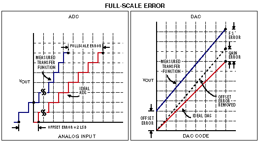
Full-scale error for an ADC and a DAC.
FS Gain Error (DACs)The full-scale gain error of an digital-to-analog converter (DAC) is the difference between the actual and the ideal output span. The actual span is determined by the output when all inputs are set to 1s, minus the output when all inputs are set to 0s. The full-scale gain error of any data converter can be affected by the choice of reference used to measure the gain error.
Gain ErrorThe gain error of an ADC or DAC indicates how well the slope of an actual transfer function matches the slope of the ideal transfer function. Gain error is usually expressed in LSB or as a percent of full-scale range (%FSR), and it can be calibrated out with hardware or in software. Gain error is the full-scale error minus the offset error.
![Gain error for an ADC</td>
</tr>
<tr>
<td colspan=]() |
