www.德州仪器.com
特性
描述
1
2
3
4
5
6
7
8
9
10
11
12
13
14
15
16
17
18
19
20
21
22
23
24
25
26
27
28
29
30
31
32
64
63
62
61
60
59
58
57
56
55
54
53
52
51
50
49
48
47
46
45
44
43
42
41
40
39
38
37
36
35
34
33
地
V
CC
V
CC
地
ENA
A1Y
A2Y
A3Y
A4Y
ENB
B1Y
B2Y
B3Y
B4Y
地
V
CC
V
CC
地
C1Y
C2Y
C3Y
C4Y
ENC
D1Y
D2Y
D3Y
D4Y
终止
地
V
CC
V
CC
地
A1A
A1B
A2A
A2B
A3A
A3B
A4A
A4B
B1A
B1B
B2A
B2B
B3A
B3B
B4A
B4B
C1A
C1B
C2A
C2B
C3A
C3B
C4A
C4B
D1A
D1B
D2A
D2B
D3A
D3B
D4A
D4B
1
2
3
4
5
6
7
8
16
15
14
13
12
11
10
9
1A
1B
2A
2B
3A
3B
4A
4B
en1,2
1Y
2Y
V
CC
地
3Y
4Y
en3,4
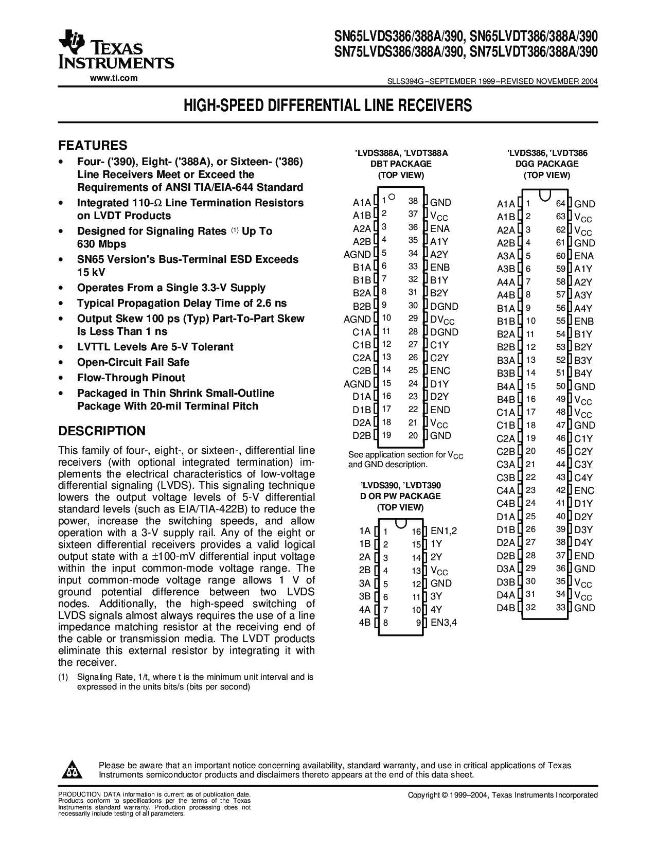
’Lvds390, ’lVDT390
d 或者 pw pACKAGE
(t运算 视图)
’Lvds386, ’lVDT386
dgg pACKAGE
(t运算 视图)
1
2
3
4
5
6
7
8
9
10
11
12
13
14
15
16
17
18
19
38
37
36
35
34
33
32
31
30
29
28
27
26
25
24
23
22
21
20
地
V
CC
ENA
A1Y
A2Y
ENB
B1Y
B2Y
DGND
DV
CC
DGND
C1Y
C2Y
ENC
D1Y
D2Y
终止
V
CC
地
A1A
A1B
A2A
A2B
AGND
B1A
B1B
B2A
B2B
AGND
C1A
C1B
C2A
C2B
AGND
D1A
D1B
D2A
D2B
’Lvds388a, ’lVDT388A
dbt pACKAGE
(t运算 视图)
看 应用 部分 为 v
CC
和 地 描述.
sn65lvds386/388a/390,sn65lvdt386/388a/390
sn75lvds386/388a/390,sn75lvdt386/388a/390
SLLS394G–SEPTEMBER1999–REVISEDNOVEMBER2004
高-speeddifferentiallinereceivers
•
四-('390),第八-('388a),orsixteen-('386)
LineReceiversMeetorExceedthe
requirementsofansitia/eia-644standard
•
integrated110-
Ω
LineTerminationResistors
onLVDTProducts
•
DesignedforSignalingRates
(1)
UpTo
630Mbps
•
sn65version'sbus-terminalesdexceeds
15kV
•
operatesfromasingle3.3-vsupply
•
typicalpropagationdelaytimeof2.6ns
•
outputskew100ps(典型值)部分-至-partskew
IsLessThan1ns
•
lvttllevelsare5-vtolerant
•
打开-circuitfailsafe
•
流动-throughpinout
•
packagedinthinshrinksmall-外形
packagewith20-milterminalpitch
thisfamilyoffour-,第八-,orsixteen-,differentialline
接受者(withoptionalintegratedtermination)im-
plementstheelectricalcharacteristicsoflow-电压
differentialsignaling(lvds).thissignalingtechnique
lowerstheoutputvoltagelevelsof5-vdifferential
standardlevels(suchaseia/tia-422b)toreducethe
电源,increasetheswitchingspeeds,andallow
operationwitha3-vsupplyrail.anyoftheeightor
sixteendifferentialreceiversprovidesavalidlogical
outputstatewitha
±
100-mvdifferentialinputvoltage
withintheinputcommon-modevoltagerange.这
inputcommon-modevoltagerangeallows1vof
groundpotentialdifferencebetweentwoLVDS
nodes.additionally,thehigh-speedswitchingof
LVDSsignalsalmostalwaysrequirestheuseofaline
impedancematchingresistoratthereceivingendof
thecableortransmissionmedia.thelvdtproducts
eliminatethisexternalresistorbyintegratingitwith
thereceiver.
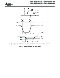
(1)signalingrate,1/t,wheretistheminimumunitintervalandis
expressedintheunitsbits/s(bitspersecond)
pleasebeawarethatanimportantnoticeconcerningavailability,standardwarranty,anduseincriticalapplicationsoftexas
instrumentssemiconductorproductsanddisclaimerstheretoappearsattheendofthisdatasheet.
productiondatainformationiscurrentasofpublicationdate.
copyright©1999–2004,texasinstrumentsincorporated
ProductsconformtospecificationsperthetermsoftheTexas
instrumentsstandardwarranty.productionprocessingdoesnot
necessarilyincludetestingofallparameters.