www.ti.com
特点
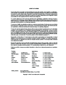
1
2
3
4
5
6
7
14
13
12
11
10
9
8
1A
1B
1Y
2A
2B
2Y
地
v
抄送
4B
4A
4Y
3B
3A
3Y
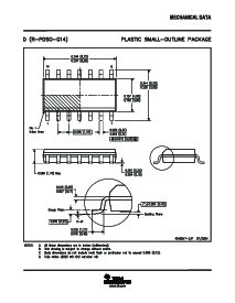
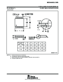
d 或 pw p组件
(top 查看)
描述/orderinginformation
一个
B
y
sn74lvc00a-q1
quadruple2-inputpositive-nandgate
SCAS703A–SEPTEMBER2003–REVISEDJUNE2005
•
qualificationinaccordancewithaec-q100
(1)
•
QualifiedforAutomotiveApplications
•
客户-specificconfigurationcontrolcan
besupportedalongwithmajor-变更
批准
•
ESDProtectionExceeds2000VPer
密耳-标准-883,method3015;exceeds200v
usingmachinemodel(c=200pf,右=0)
•
operatesfrom2vto3.6v
•
inputsacceptvoltagesto5.5v
•
maxt
pd
of4.3nsat3.3v
•
TypicalV
olp
(outputgroundbounce)&指示灯;0.8v
atV
抄送
=3.3v,t
一个
=25°C
•
TypicalV
OHV
(outputv
哦
下冲)>2vat
v
抄送
=3.3v,t
一个
=25°C
(1)contactfactoryfordetails.q100qualificationdataavailable
onrequest.
thesn74lvc00a-q1quadruple2-inputpositive-nandgateisdesignedfor2.7-vto3.6-vv
抄送
操作.
ThedeviceperformstheBooleanfunctionY=A
⋅
bory=a+binpositivelogic.
inputscanbedrivenfromeither3.3-vor5-vdevices.thisfeatureallowstheuseofthisdeviceasatranslatorin
amixed3.3-v/5-vsystemenvironment.
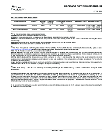
ORDERINGINFORMATION
t
一个
包装
(1)
orderablepartnumbertop-sidemarking
SOIC–DReelof2500SN74LVC00AQDRQ1LVC00AQ
–40°Cto125°C
TSSOP–PWReelof2000SN74LVC00AQPWRQ1LVC00AQ
(1)packagedrawings,标准包装数量,thermaldata,符号化,andpcbdesignguidelinesareavailableat
www.ti.com/sc/包装.
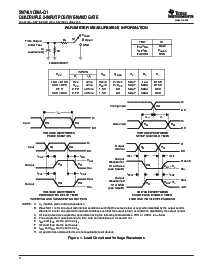
FUNCTIONTABLE
(eachgate)
输入
输出
y
AB
HHL
LXH
XLH
logicdiagram,eachgate(positivelogic)
pleasebeawarethatanimportantnoticeconcerningavailability,标准保修,anduseincriticalapplicationsoftexas
instrumentssemiconductorproductsanddisclaimerstheretoappearsattheendofthisdatasheet.
productiondatainformationiscurrentasofpublicationdate.
copyright©2003–2005,texasinstrumentsincorporated
ProductsconformtospecificationsperthetermsoftheTexas
instrumentsstandardwarranty.productionprocessingdoesnot
必要包括测试所有参数.