www.德州仪器.com
特性
1
2
3
4
5
6
7
8
9
10
20
19
18
17
16
15
14
13
12
11
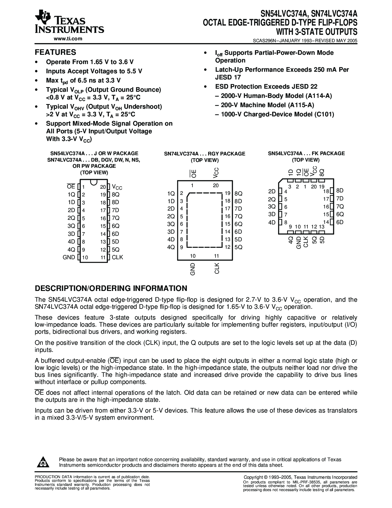
OE
1Q
1D
2D
2Q
3Q
3D
4D
4Q
地
V
CC
8Q
8D
7D
7Q
6Q
6D
5D
5Q
CLK
SN54LVC374A . . . j 或者 w pACKAGE
SN74LVC374A . . . db, dgv, dw, n, ns,
或者 pw pACKAGE
(t运算 视图)
SN54LVC374A . . . fk pACKAGE
(t运算 视图)
3 2 1 20 19
9 10 11 12 13
4
5
6
7
8
18
17
16
15
14
1D
1Q
OE
5Q
5D
8Q
4Q
地
CLK
V
CC
8D
7D
7Q
6Q
6D
SN74LVC374A . . . rgy pACKAGE
(t运算 视图)
1 20
10 11
2
3
4
5
6
7
8
9
19
18
17
16
15
14
13
12
8Q
8D
7D
7Q
6Q
6D
5D
5Q
1Q
1D
2D
2Q
3Q
3D
4D
4Q
CLK
V
地
CC
OE
2D
2Q
3Q
3D
4D
描述/orderinginformation
sn54lvc374a,sn74lvc374a
octaledge-triggeredd-typeflip-flops
with3-stateoutputs
SCAS296N–JANUARY1993–REVISEDMAY2005
•
I
止
supportspartial-电源-downmode
运作
•
operatefrom1.65vto3.6v
•
获得-upperformanceexceeds250maper
•
inputsacceptvoltagesto5.5v
JESD17
•
Maxt
pd
of6.5nsat3.3v
•
ESDProtectionExceedsJESD22
•
TypicalV
OLP
(outputgroundbounce)
–2000-vhuman-bodymodel(a114-一个)
<0.8vatv
CC
=3.3v,t
一个
=25°C
–200-vmachinemodel(a115-一个)
•
TypicalV
OHV
(outputv
OH
undershoot)
>2vatv
CC
=3.3v,t
一个
=25°c–1000-vcharged-devicemodel(c101)
•
supportmixed-modesignaloperationon
allports(5-vinput/outputvoltage
with3.3-vv
CC
)
thesn54lvc374aoctaledge-triggeredd-typeflip-flopisdesignedfor2.7-vto3.6-vv
CC
运作,andthe
sn74lvc374aoctaledge-triggeredd-typeflip-flopisdesignedfor1.65-vto3.6-vv
CC
运作.
thesedevicesfeature3-stateoutputsdesignedspecificallyfordrivinghighlycapacitiveorrelatively
低-impedanceloads.thesedevicesareparticularlysuitableforimplementingbufferregisters,输入/输出(i/o)
端口,bidirectionalbusdrivers,andworkingregisters.
onthepositivetransitionoftheclock(clk)输入,theqoutputsaresettothelogiclevelssetupatthedata(d)
输入.
abufferedoutput-使能(oe)inputcanbeusedtoplacetheeightoutputsineitheranormallogicstate(highor
lowlogiclevels)orthehigh-impedancestate.inthehigh-impedancestate,theoutputsneitherloadnordrivethe
buslinessignificantly.thehigh-impedancestateandincreaseddriveprovidethecapabilitytodrivebuslines
withoutinterfaceorpullupcomponents.
oedoesnotaffectinternaloperationsofthelatch.olddatacanberetainedornewdatacanbeenteredwhile
theoutputsareinthehigh-impedancestate.
inputscanbedrivenfromeither3.3-vor5-vdevices.thisfeatureallowstheuseofthesedevicesastranslators
inamixed3.3-v/5-vsystemenvironment.
pleasebeawarethatanimportantnoticeconcerningavailability,standardwarranty,anduseincriticalapplicationsoftexas
instrumentssemiconductorproductsanddisclaimerstheretoappearsattheendofthisdatasheet.
productiondatainformationiscurrentasofpublicationdate.
copyright©1993–2005,texasinstrumentsincorporated
ProductsconformtospecificationsperthetermsoftheTexas
onproductscomplianttomil-prf-38535,allparametersare
instrumentsstandardwarranty.productionprocessingdoesnot
testedunlessotherwisenoted.onallotherproducts,生产
necessarilyincludetestingofallparameters.
processingdoesnotnecessarilyincludetestingofallparameters.