www.德州仪器.com
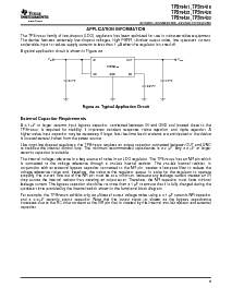
BoardLayoutRecommendationtoImprovePSRRandNoisePerformance
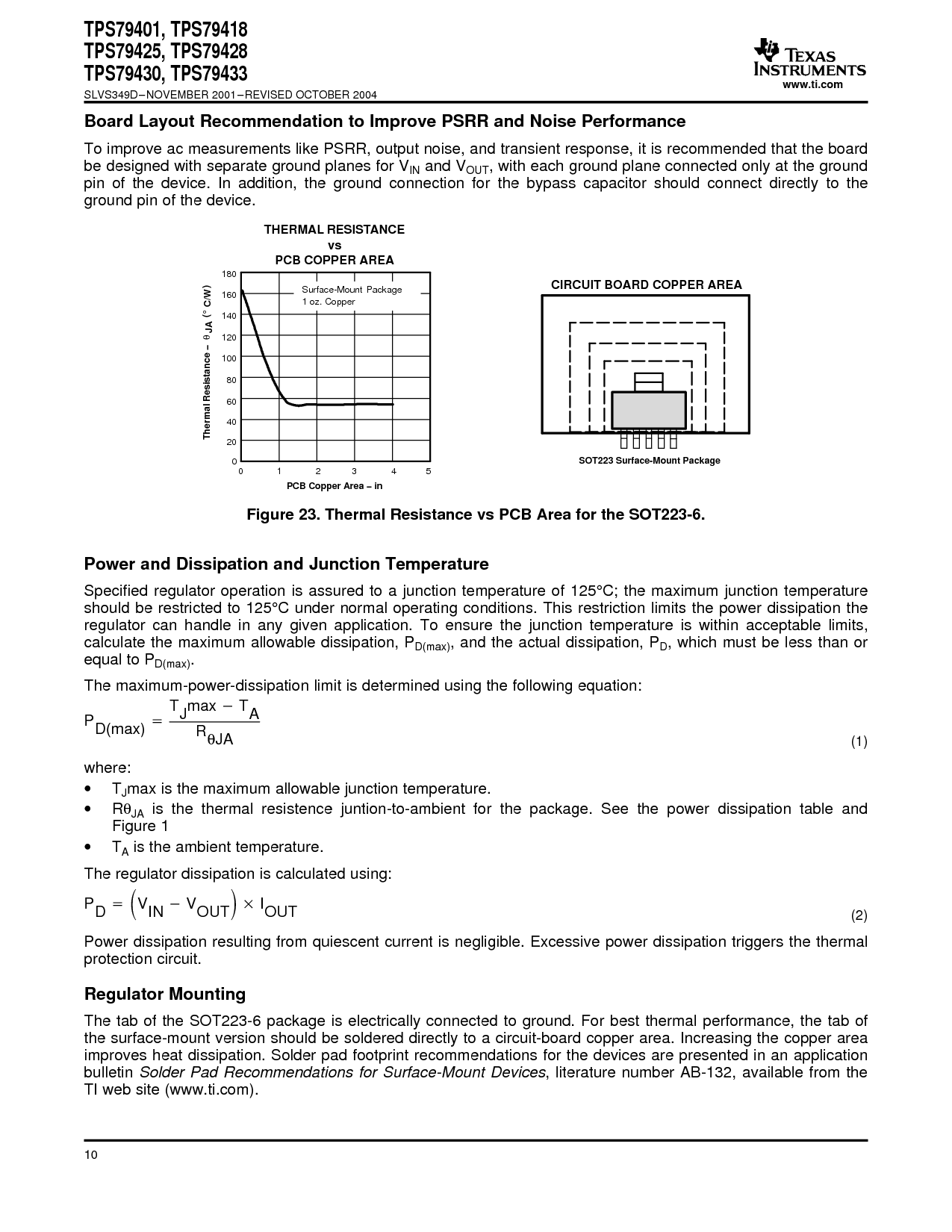
pcb 铜 范围 − 在
100
80
40
0 1 2 3
热的 阻抗 −
120
140
热的RESISTANCE
vs
pcb 铜 范围
180
4 5
160
60
0
20
JA
θ
c/w
°
( )
表面-挂载包装
1 oz. 铜
电路板 铜 范围
SOT223表面-挂载 包装
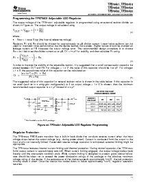
PowerandDissipationandJunctionTemperature
P
d(最大值)
T
J
最大值
T
一个
R
θ
JA
(1)
P
D
V
在
V
输出
I
输出
(2)
RegulatorMounting
tps79401,tps79418
tps79425,tps79428
tps79430,tps79433
SLVS349D–NOVEMBER2001–REVISEDOCTOBER2004
toimproveacmeasurementslikepsrr,outputnoise,andtransientresponse,itisrecommendedthattheboard
bedesignedwithseparategroundplanesforV
在
andV
输出
,witheachgroundplaneconnectedonlyattheground
pinofthedevice.inaddition,thegroundconnectionforthebypasscapacitorshouldconnectdirectlytothe
groundpinofthedevice.
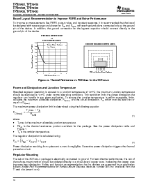
figure23.thermalresistancevspcbareaforthesot223-6.
Specifiedregulatoroperationisassuredtoajunctiontemperatureof125
°
c;themaximumjunctiontemperature
shouldberestrictedto125
°
cundernormaloperatingconditions.thisrestrictionlimitsthepowerdissipationthe
regulatorcanhandleinanygivenapplication.toensurethejunctiontemperatureiswithinacceptablelimits,
calculatethemaximumallowabledissipation,p
d(最大值)
,andtheactualdissipation,p
D
,whichmustbelessthanor
equaltoP
d(最大值)
.
themaximum-电源-dissipationlimitisdeterminedusingthefollowingequation:
在哪里:
•
T
J
maxisthemaximumallowablejunctiontemperature.
•
R
θ
JA
isthethermalresistencejuntion-至-ambientforthepackage.seethepowerdissipationtableand
Figure1
•
T
一个
istheambienttemperature.
theregulatordissipationiscalculatedusing:
powerdissipationresultingfromquiescentcurrentisnegligible.excessivepowerdissipationtriggersthethermal
protectioncircuit.
thetabofthesot223-6packageiselectricallyconnectedtoground.forbestthermalperformance,thetabof
thesurface-mountversionshouldbesoldereddirectlytoacircuit-boardcopperarea.increasingthecopperarea
improvesheatdissipation.solderpadfootprintrecommendationsforthedevicesarepresentedinanapplication
公告
solderpadrecommendationsforsurface-mountdevices
,literaturenumberab-132,availablefromthe
tiwebsite(www.德州仪器.com).
10