www.德州仪器.com
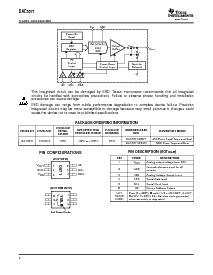
V
DD
SCLA0
地
输出
缓存区
电源-向下
控制 逻辑
电阻
网络
ref (+) ref(−)
8-位
DAC
I
2
C
控制
逻辑
DAC
寄存器
电源-在
重置
V
输出
SDA
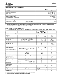
PINCONFIGURATIONS
A0
SCL
SDA
6
5
4
1
2
3
V
输出
地
V
DD
D571
1
2
3
6
5
4
YMLL
(t运算 视图)
(bottom 视图)
lot trace 代号
DAC5571
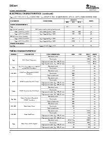
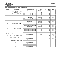
SLAS405–DECEMBER2003
thisintegratedcircuitcanbedamagedbyesd.texasinstrumentsrecommendsthatallintegrated
circuitsbehandledwithappropriateprecautions.failuretoobserveproperhandlingandinstallation
procedurescancausedamage.
esddamagecanrangefromsubtleperformancedegradationtocompletedevicefailure.精确
integratedcircuitsmaybemoresusceptibletodamagebecauseverysmallparametricchangescould
causethedevicenottomeetitspublishedspecifications.
包装/orderinginformation
包装
specifiedtem-packageorderingnum-
productpackagedesig-transportmedia
PERATURERANGEMARKINGBER
NATOR
DAC5571IDBVT250PieceSmallTapeandReel
dac5571sot23-6dbv-40
°
Cto+105
°
CD571
DAC5571IDBVR3000PieceTapeandReel
pindescription(sot23-6)
PINNAMEDESCRIPTION
1V
输出
AnalogoutputvoltagefromDAC
Groundreferencepointforall
2GND
电路系统
3V
DD
AnalogVoltageSupplyInput
4SDASerialDataInput
5SCLSerialClockInput
6A0DeviceAddressSelect
LOT
Y
ear(3=2003);
M
onth(1–9=jan–sep;一个=oct,
traceb=十一月,c=dec);
LL
–Randomcodegenerated
代号:whenassemblyisrequested
2