www.德州仪器.com
3
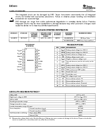
A3
A2
A1
1
2
3
4
5
6
7
8
16
15
14
1
12
11
10
9
V
输出
一个
V
输出
B
V
REF
H
V
DD
V
REF
L
地
V
输出
C
V
输出
D
A0
IOV
DD
SDA
SCL
LDAC
DAC6573
ABSOLUTEMAXIMUMRATINGS
(1)
DAC6573
SLAS402–NOVEMBER2003
thisintegratedcircuitcanbedamagedbyesd.texasinstrumentsrecommendsthatallintegrated
circuitsbehandledwithappropriateprecautions.failuretoobserveproperhandlingandinstallation
procedurescancausedamage.
esddamagecanrangefromsubtleperformancedegradationtocompletedevicefailure.精确
integratedcircuitsmaybemoresusceptibletodamagebecauseverysmallparametricchangescould
causethedevicenottomeetitspublishedspecifications.
包装/orderinginformation
PRODUCTPACKAGEPACKAGESPECIFICATIONPACKAGEORDERINGTRANSPORTMEDIA
DRAWINGTEMPERATUREMARKINGNUMBER
NUMBERRANGE
dac657316-tssoppw–40
°
CTO+105
°
CD6573IDAC6573IPW90PieceTube
DAC6573IPWR2000PieceTapeandReel
PWPACKAGE
PINDESCRIPTIONS
(topview)
PINNAMEDESCRIPTION
1V
输出
AAnalogoutputvoltagefromDACA
2V
输出
BAnalogoutputvoltagefromDACB
3V
REF
HPositivereferencevoltageinput
4V
DD
Analogvoltagesupplyinput
5V
REF
LNegativereferencevoltageinput
Groundreferencepointforallcircuitryonthe
6GND
部分
7V
输出
CAnalogoutputvoltagefromDACC
8V
输出
DAnalogoutputvoltagefromDACD
9ldach/wsynchronousv
输出
更新
10SCLSerialclockinput
11SDASerialdatainput
12IOV
DD
i/ovoltagesupplyinput
13a0deviceaddressselect-i
2
C
14a1deviceaddressselect-i
2
C
15a2deviceaddressselect-扩展
16a3deviceaddressselect-扩展
V
DD
tognd–0.3vto+6v
digitalinputvoltagetognd–0.3vtov
DD
+0.3v
V
输出
tognd–0.3vtov
DD
+0.3v
Operatingtemperaturerange–40
°
Cto+105
°
C
Storagetemperaturerange–65
°
Cto+150
°
C
junctiontemperaturerange(t
J
最大值)+150
°
C
powerdissipationthermalimpedance(
R
Θ
JA
)161
°
c/w
thermalimpedance(r
Θ
JC
)29
°
c/w
leadtemperature,solderingvaporphase(60s)215
°
C
infrared(15s)220
°
C
(1)stressesabovethoselistedunderabsolutemaximumratingsmaycausepermanentdamagetothedevice.exposuretoabsolute
maximumconditionsforextendedperiodsmayaffectdevicereliability.
2