www.德州仪器.com
产品 预告(展)
APPLICATIONINFORMATION
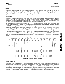
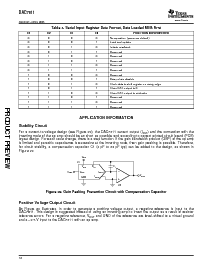
StabilityCircuit
I
OUT1
V
输出
R
FB
C
1
地
V
DD
V
DD
U1
U2
V
REF
V
REF
I
OUT2
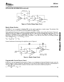
PositiveVoltageOutputCircuit
DAC7811
SBAS337–APRIL2005
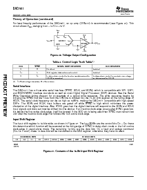
table3.serialinputregisterdataformat,dataloadedmsbfirst
C3C2C1C0FUNCTIONIMPLEMENTED
0000nooperation(电源-ondefault)
0001Loadandupdate
0010Initiatereadback
0011Reserved
0100Reserved
0101Reserved
0110Reserved
0111Reserved
1000Reserved
1001daisy-chaindisable
1010Clockdatatoshiftregisteronrisingedge
1011ClearDACoutputto0
1100ClearDACoutputtomidscale
1101Reserved
1110Reserved
1111Reserved
foracurrent-至-voltagedesign(seefigure29),thedac7811currentoutput(i
输出
)andtheconnectionwiththe
invertingnodeoftheopampshouldbeasshortaspossibleandaccordingtocorrectprintedcircuitboard(pcb)
layoutdesign.foreachcodechange,thereisastepfunction.ifthegainbandwidthproduct(gbp)oftheopamp
islimitedandparasiticcapacitanceisexcessiveattheinvertingnode,thengainpeakingispossible.因此,
forcircuitstability,acompensationcapacitorc1(4pfto20pftyp)canbeaddedtothedesign,asshownin
figure29.
figure29.gainpeakingpreventioncircuitwithcompensationcapacitor
asfigure30illustrates,inordertogenerateapositivevoltageoutput,anegativereferenceisinputtothe
dac7811.thisdesignissuggestedinsteadofusinganinvertingamptoinverttheoutputasaresultofresistor
toleranceerrors.foranegativereference,v
输出
andgndofthereferencearelevel-shiftedtoavirtualground
anda–2.5vinputtothedac7811withanopamp.
12