www.德州仪器.com
产品 预告(展)
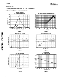
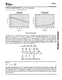
0
−
0.2
−
0.4
−
0.6
−
0.8
−
1.0
−
1.2
−
1.4
−
1.6
−
1.8
−
2.0
−
40
−
20 0 20 40 60 80 100 120
增益 错误 (mv)
温度 (
c)
V
REF
= +10V
1.6
1.4
1.2
1.0
0.8
0.6
0.4
0.2
0
−
40
−
20 0 20 40 60 80 100 120
输出 泄漏 (na)
温度 (
c)
V
REF
= +10V
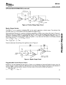
TheoryofOperation
R R R R
2R 2R 2R 2R
R
FB
I
OUT2
I
输出 1
2R
V
REF
DB0
(lsb)
DB9DB10DB11
(msb)
V
输出
V
REF
代号
4096
(1)
DAC7811
SBAS337–APRIL2005
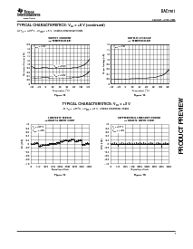
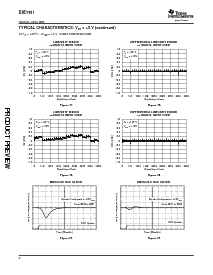
typicalcharacteristics:v
DD
=+3v(持续)
AtT
一个
=+25
°
c,+v
DD
=+3v,unlessotherwisenoted.
GAINERROROUTPUTLEAKAGE
vsTEMPERATUREvsTEMPERATURE
figure23.figure24.
thedac7811isasinglechannelcurrentoutput,12-bitdigital-至-analogconverter(dac).thearchitecture,
illustratedinfigure25,isanr-2rladderconfigurationwiththethreemsbssegmented.each2rlegofthe
ladderiseitherswitchedtoI
OUT1
ortheI
OUT2
终端.thei
OUT1
terminaloftheDACisheldatavirtualGND
potentialbytheuseofanexternali/vconverteropamp.ther-2rladderisconnectedtoanexternalreference
inputV
REF
thatdeterminesthedacfull-scalecurrent.ther-2rladderpresentsacodeindependentload
impedancetotheexternalreferenceof10k
Ω±
20%.theexternalreferencevoltagecanvaryinarangeof–15v
to+15v,thusprovidingbipolari
输出
currentoperation.byusinganexternali/vconverterandthedac7811r
FB
电阻,outputvoltagerangesof-v
REF
toV
REF
canbegenerated.
figure25.equivalentr-2rdaccircuit
whenusinganexternali/vconverterandthedac7811r
FB
电阻,thedacoutputvoltageisgivenby
equation1:
EachDACcodedeterminesthe2RlegswitchpositiontoeitherGNDorI
输出
.becausethedacoutput
impedanceasseenlookingintotheI
OUT1
terminalchangesversuscode,theexternali/vconverternoisegainwill
alsochange.becauseofthis,theexternali/vconverteropampmusthaveasufficientlylowoffsetvoltagesuch
thattheamplifieroffsetisnotmodulatedbytheDACI
OUT1
terminalimpedancechange.externalopampswith
largeoffsetvoltagescanproduceINLerrorsinthetransferfunctionoftheDAC7811duetooffsetmodulation
versusdaccode.
9