www.德州仪器.com
APPLICATIONINFORMATION
TPS730xx
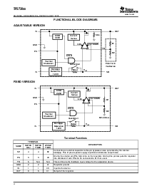
GNDEN NR
在 输出
V
在
V
输出
V
在
V
输出
2.2
µ
F
0.01
µ
F
(1)
0.1
µ
F
便条: (1) 这个 电容 是 optional.
ExternalCapacitorRequirements
BoardLayoutRecommendationtoImprovePSRRandNoisePerformance
TPS730xx
SBVS054E–NOVEMBER2004–REVISEDAUGUST2005
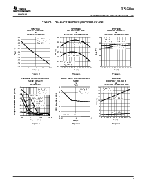
thetps730xxfamilyoflow-落后(ldo)regulatorshasbeenoptimizedforuseinnoise-敏感的
电池-operatedequipment.thedevicefeaturesextremelylowdropoutvoltages,highpsrr,ultralowoutput
噪音,lowquiescentcurrent(170µatypically),andenable-inputtoreducesupplycurrentstolessthan1µa
whentheregulatoristurnedoff.
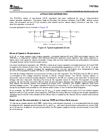
AtypicalapplicationcircuitisshowninFigure16.
figure16.typicalapplicationcircuit
a0.1-µforlargerceramicinputbypasscapacitor,connectedbetweeninandgndandlocatedclosetothe
tps730xx,isrequiredforstabilityandimprovestransientresponse,noiserejection,andripplerejection.一个
高等级的-valueinputcapacitormaybenecessaryiflarge,快-上升-timeloadtransientsareanticipatedorthedevice
islocatedseveralinchesfromthepowersource.
likemostlowdropoutregulators,thetps730xxrequiresanoutputcapacitorconnectedbetweenoutandgnd
tostabilizetheinternalcontrolloop.theminimumrecommendedcapacitanceis2.2µf.any2.2-µforlarger
ceramiccapacitorissuitable,providedthecapacitancedoesnotvarysignificantlyovertemperature.ifload
currentisnotexpectedtoexceed100ma,a1.0-µfceramiccapacitorcanbeused.
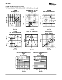
theinternalvoltagereferenceisakeysourceofnoiseinanldoregulator.thetps730xxhasannrpinwhich
isconnectedtothevoltagereferencethrougha250-k
Ω
internalresistor.the250-k
Ω
internalresistor,在
conjunctionwithanexternalbypasscapacitorconnectedtothenrpin,createsalowpassfiltertoreducethe
voltagereferencenoiseand,因此,thenoiseattheregulatoroutput.inorderfortheregulatortooperate
合适的,thecurrentflowoutofthenrpinmustbeataminimum,becauseanyleakagecurrentcreatesanir
dropacrosstheinternalresistorthuscreatinganoutputerror.因此,thebypasscapacitormusthave
minimalleakagecurrent.thebypasscapacitorshouldbenomorethan0.1-µftoensurethatitisfullycharged
duringthequickstarttimeprovidedbytheinternalswitchshownintheFunctionalBlockDiagrams
asanexample,thetps73018exhibitsonly23µv
RMS
ofoutputvoltagenoiseusinga0.01-µfceramicbypass
capacitoranda2.2-µfceramicoutputcapacitor.notethattheoutputstartsupslowerasthebypasscapacitance
increasesduetotherctimeconstantatthenrpinthatiscreatedbytheinternal250-k
Ω
resistorandexternal
电容.
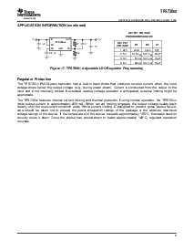
toimproveacmeasurementslikepsrr,outputnoise,andtransientresponse,itisrecommendedthattheboard
bedesignedwithseparategroundplanesforV
在
andV
输出
,witheachgroundplaneconnectedonlyatthegnd
pinofthedevice.inaddition,thegroundconnectionforthebypasscapacitorshouldconnectdirectlytothegnd
pinofthedevice.
7