www.德州仪器.com
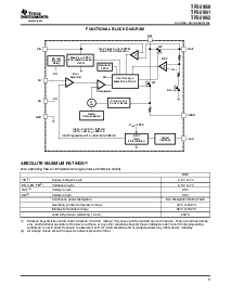
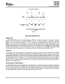
比较器
错误
放大器
FB
PGND
Q1
输出
VIN
EN
Q2
EN
ILED
地
EN
OVP
EN
EN
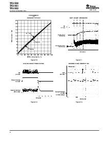
50-ms
Turnoff
延迟
偏差 v
ref
= 1.22 v
热的 关闭
UVLO
前-承担 电流/pwm
短的-电路 发现
SW
V
ref
振荡器
1 mhz
控制 逻辑
门 驱动 电路
电流 限制
电流 sense
Ramp
补偿
Σ
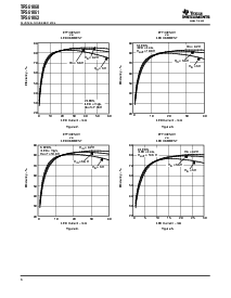
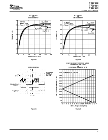
iled = 高 v
FB
= 250 mv
iled = 低 v
FB
= 500 mv
iled 编写程序 v
FB
= 15.6 mv 至 500 mv
V
ref
= 1.22 v
5-位
DAC
15.6 mv/步伐
数字的
接口
ABSOLUTEMAXIMUMRATINGS
(1)
TPS61060
TPS61061
TPS61062
SLVS538–NOVEMBER2004
FUNCTIONALBLOCKDIAGRAM
overoperatingfree-airtemperaturerange(unlessotherwisenoted)
单位
VIN
(2)
supplyvoltagesonpin–0.3vto7v
en,iled,fb
(2)
voltagesonpins–0.3vto7v
输出
(2)
Voltageonpin33V
SW
(2)
Voltageonpin33V
ContinuouspowerdissipationSeeDissipationRatingTable
Operatingjunctiontemperaturerange–40
°
Cto150
°
C
Storagetemperaturerange–55
°
Cto150
°
C
leadtemperature(焊接,10sec)260
°
C
(1)stressesbeyondthoselistedunder"absolutemaximumratings"maycausepermanentdamagetothedevice.thesearestressratings
仅有的,andfunctionaloperationofthedeviceattheseoranyotherconditionsbeyondthoseindicatedunder"recommendedoperating
情况"isnotimplied.exposuretoabsolute-最大-ratedconditionsforextendedperiodsmayaffectdevicereliability.
(2)allvoltagevaluesarewithrespecttonetworkgroundterminal.
3