www.德州仪器.com
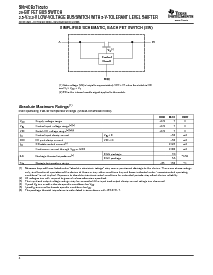
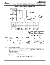
simplifiedschematic,eachfetswitch(sw)
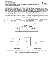
一个
EN
(2)
B
控制
电路
V
G
(1)
(1) 门 电压 (v
G
) 是 equal 至 大概 v
CC
+ v
T
当 这 转变 是在
和V
I
>
V
CC
+ v
T
.
(2) en 是 这 内部的 使能 信号 应用 至 这 转变.
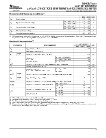
AbsoluteMaximumRatings
(1)
SN74CB3T16210
20-bitfetbusswitch
2.5-v/3.3-vlow-voltagebusswitchwith5-v-tolerantlevelshifter
SCDS156A–OCTOBER2003–REVISEDMARCH2005
overoperatingfree-airtemperaturerange(unlessotherwisenoted)
MINMAXUNIT
V
CC
supplyvoltagerange–0.57v
V
在
Controlinputvoltagerange
(2)(3)
–0.57v
V
i/o
switchi/ovoltagerange
(2)(3)(4)
–0.57v
I
IK
ControlinputclampcurrentV
在
<0–50ma
I
i/ok
i/oportclampcurrentv
i/o
<0–50ma
I
IO
在-stateswitchcurrent
(5)
±
128mA
ContinuouscurrentthroughV
CC
orGND
±
100mA
DGGpackage70
θ
JA
Packagethermalimpedance
(6)
°
c/w
DGVpackage58
T
stg
Storagetemperaturerange–65150
°
C
(1)stressesbeyondthoselistedunder"absolutemaximumratings"maycausepermanentdamagetothedevice.thesearestressratings
仅有的,andfunctionaloperationofthedeviceattheseoranyotherconditionsbeyondthoseindicatedunder"recommendedoperating
情况"isnotimplied.exposuretoabsolute-最大-ratedconditionsforextendedperiodsmayaffectdevicereliability.
(2)allvoltagesarewithrespecttogroundunlessotherwisespecified.
(3)theinputandoutputvoltageratingsmaybeexceedediftheinputandoutputclamp-currentratingsareobserved.
(4)v
I
andV
O
areusedtodenotespecificconditionsforV
i/o
.
(5)i
I
andI
O
areusedtodenotespecificconditionsforI
i/o
.
(6)thepackagethermalimpedanceiscalculatedinaccordancewithjesd51-7.
4