www.德州仪器.com
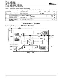
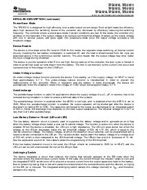
DGS
(顶 视图)
DRC
(顶 视图)
1
2
3
4
5
10
9
8
7
6
EN
竞赛
FB
地
VOUT
LBO
LBI
ADEN
SW
VBAT
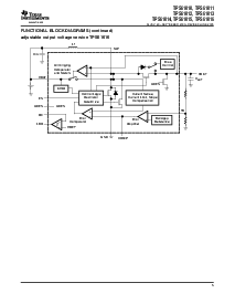
FB
地
VOUT
VBA
T
LBI
竞赛
SW
ADEN
EN
LBO
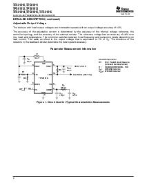
DETAILEDDESCRIPTION
ControllerCircuit
SynchronousRectifier
tps61010,tps61011
tps61012,tps61013
tps61014,tps61015,tps61016
SLVS314D–SEPTEMBER2000–REVISEDJUNE2005
TerminalFunctions
终端
i/odescription
DRGDRC
名字
非.非.
autodischargeinput.theautodischargefunctionisenabledifthispinisconnectedtovbat,itisdisabled
ADEN88I
ifadenistiedtognd.
comp22icompensationoferroramplifier.connectanr/c/cnetworktosetfrequencyresponseofcontrolloop.
1ichip-enableinput.theconverterisswitchedonifthispinissethigh,itisswitchedoffifthispinis
EN1
connectedtognd.
feedbackinputforadjustableoutputvoltageversiontps61010.outputvoltageisprogrammed
fb33idependingontheoutputvoltagedividerconnectedthere.forthefixedoutputvoltageversions,leave
fb-pinunconnected.
GND44Ground
低-batterydetectorinput.alowbatterywarningisgeneratedatlbowhenthevoltageonlbidrops
lbi99ibelowthethresholdof500mv.connectlbitogndorvbatifthelow-batterydetectorfunctionisnot
使用.donotleavethispinfloating.
打开-drainlow-batterydetectoroutput.thispinispulledlowifthevoltageonlbidropsbelowthe
LBO1010O
thresholdof500mv.apullupresistormustbeconnectedbetweenlboandvout.
sw77iswitchinputpin.theinductorisconnectedtothispin.
vout55ooutputvoltage.internalresistordividersetsregulatedoutputvoltageinfixedoutputvoltageversions.
VBAT66ISupplypin
thedeviceisbasedonacurrent-modecontroltopologyusingaconstantfrequencypulse-widthmodulatorto
regulatetheoutputvoltage.thecontrollerlimitsthecurrentthroughthepowerswitchonapulsebypulsebasis.
thecurrent-sensingcircuitisintegratedinthedevice,因此,noadditionalcomponentsarerequired.dueto
thenatureoftheboostconvertertopologyusedhere,thepeakswitchcurrentisthesameasthepeakinductor
电流,whichwillbelimitedbytheintegratedcurrentlimitingcircuitsundernormaloperatingconditions.
thecontrolloopmustbeexternallycompensatedwithanr-c-cnetworkconnectedtothecomp-管脚.
thedeviceintegratesann-channelandap-channelmosfettransistortorealizeasynchronousrectifier.那里
isnoadditionalschottkydioderequired.becausethedeviceusesaintegratedlowr
ds(在)
PMOSswitchfor
整流,thepowerconversionefficiencyreaches95%.
aspecialcircuitisappliedtodisconnecttheloadfromtheinputduringshutdownoftheconverter.inconventional
synchronousrectifiercircuits,thebackgatediodeofthehigh-sidepmosisforwardbiasedinshutdownand
allowscurrentflowingfromthebatterytotheoutput.thisdevice,不管怎样,usesaspecialcircuittodisconnect
thebackgatediodeofthehigh-sidepmosandso,disconnectstheoutputcircuitryfromthesourcewhenthe
regulatorisnotenabled(en=低).
thebenefitofthisfeatureforthesystemdesignengineer,isthatthebatteryisnotdepletedduringshutdownof
theconverter.所以,noadditionalefforthastobemadebythesystemdesignertoensuredisconnectionofthe
batteryfromtheoutputoftheconverter.因此,designperformancewillbeincreasedwithoutadditionalcosts
andboardspace.
6