www.德州仪器.com
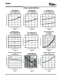
COMPONENTSELECTION
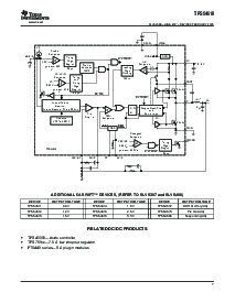
INPUTFILTER
FEEDBACKCIRCUIT
OPERATINGFREQUENCY
R
500 kHz
切换 频率
100 [k
]
(1)
OUTPUTFILTER
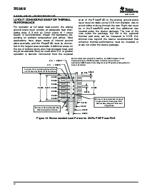
PCBLAYOUT
TPS54610
SLVS398E–JUNE2001–REVISEDFEBRUARY2005
capacitorconnections,thevinpins,andthe
tps54610groundpins.theminimumrecommended
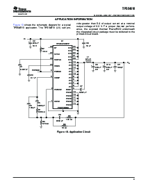
Thevaluesforthecomponentsusedinthisdesign
bypasscapacitanceis10-mfceramiccapacitorwith
examplewereselectedusingtheSWIFTdesigner
aX5RorX7Rdielectricandtheoptimumplacement
softwaretool.swiftdesignerprovidesacomplete
isclosesttothevinpinsandthepgndpins.
designenvironmentfordevelopingdc-dcconverters
usingthetps54610.thetps54610hastwointernalgrounds(analogand
电源).insidethetps54610,theanaloggroundties
toallofthenoisesensitivesignals,whilethepower
groundtiestothenoisierpowersignals.噪音
theinputtothecircuitisanominal5vdc.theinput
injectedbetweenthetwogroundscandegradethe
filterc2isa220-µfposcapcapacitor,witha
performanceofthetps54610,particularlyathigher
maximumallowableripplecurrentof3a.c8provides
outputcurrents.不管怎样,groundnoiseonananalog
highfrequencydecouplingoftheTPS54610fromthe
groundplanecanalsocauseproblemswithsomeof
inputsupplyandmustbelocatedascloseas
thecontrolandbiassignals.forthesereasons,
possibletothedevice.ripplecurrentiscarriedin
separateanalogandpowergroundtracesarerec-
bothc2andc8,andthereturnpathtopgndmust
ommended.thereisanareaofgroundonthetop
avoidthecurrentcirculatingintheoutputcapacitors
layerdirectlyundertheic,withanexposedareafor
c9andc10.
connectiontothepowerpad.useviastoconnect
thisgroundareatoanyinternalgroundplanes.
Additionalviasarealsousedatthegroundsideof
theinputandoutputfiltercapacitors.theagndand
TheresistordividernetworkofR3andR4setsthe
PGNDpinsaretiedtothePCBgroundbyconnecting
outputvoltageforthecircuitat3.3v.r4,alongwith
themtothegroundareaunderthedeviceasshown.
r1,r5,c3,c5,andc6formtheloopcompensation
Theonlycomponentsthattiedirectlytothepower
networkforthecircuit.forthisdesign,atype3
groundplanearetheinputcapacitors,theoutput
topologyisused.
电容,theinputvoltagedecouplingcapacitor,
andthepgndpinsofthetps54610.useaseparate
widetracefortheanaloggroundsignalpath.这
intheapplicationcircuit,the350khzoperationis
analoggroundisusedforthevoltagesetpoint
selectedbyleavingrtandsyncopen.连接
分隔物,timingresistorrt,慢-startcapacitorand
a180k
Ω
to68k
Ω
resistorbetweenrt(pin28)和
biascapacitorgrounds.connectthistracedirectlyto
analoggroundcanbeusedtosettheswitching
agnd(pin1).
frequencyto280khzto700khz.tocalculatethert
ThePHpinsaretiedtogetherandroutedtothe
电阻,usetheequationbelow:
outputinductor.sincethephconnectionisthe
switchingnode,theinductorislocatedclosetothe
phpins.theareaofthepcbconductorisminimized
topreventexcessivecapacitivecoupling.connectthe
bootcapacitorbetweenthephasenodeandthe
bootpinasshown.keepthebootcapacitorcloseto
theoutputfilteriscomposedofa4.7-µhinductor
theicandminimizetheconductortracelengths.
andtwo470-µfcapacitors.theinductorisalowdc
阻抗(12m
Ω
)类型,coiltronicsup3b-4r7.这
connecttheoutputfiltercapacitor(s)asshownbe-
capacitorsusedare4-vposcaptypeswitha
tweenthevouttraceandpgnd.itisimportantto
maximumesrof0.040
Ω
.thefeedbackloopis
keeptheloopformedbythephpins,lout,cout
compensatedsothattheunitygainfrequencyis
andpgndassmallaspractical.
approximately25khz.
PlacethecompensationcomponentsfromtheVOUT
tracetothevsenseandcomppins.donotplace
thesecomponentstooclosetothephtrace.dueto
thesizeoftheicpackageandthedevicepin-输出,
Figure11showsageneralizedPCBlayoutguidefor
theymustberoutedclose,butmaintainasmuch
thetps54610.
separationaspossiblewhilestillkeepingthelayout
TheVINpinsareconnectedtogetheronthe
紧凑的.
打印-circuitboard(pcb)andbypassedwitha
ConnectthebiascapacitorfromtheVBIASpinto
低-esrceramic-bypasscapacitor.careshouldbe
analoggroundusingtheisolatedanalogground
takentominimizetheloopareaformedbythebypass
查出.ifaslow-startcapacitororrtresistorisused,
orifthesyncpinisusedtoselect350-khz
operatingfrequency,connectthemtothistrace.
10