www.德州仪器.com
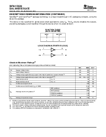
描述/orderinginformation(持续)
1A 1Y
1 6
2A 2Y
3 4
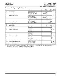
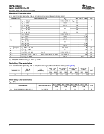
AbsoluteMaximumRatings
(1)
SN74LVC2G04
DUALINVERTERGATE
SCES195J–APRIL1999–REVISEDJULY2005
nanostar™andnanofree™packagetechnologyisamajorbreakthroughinicpackagingconcepts,usingthe
dieasthepackage.
thisdeviceisfullyspecifiedforpartial-电源-downapplicationsusingi
止
.thei
止
circuitrydisablestheoutputs,
preventingdamagingcurrentbackflowthroughthedevicewhenitispowereddown.
FUNCTIONTABLE
(eachinverter)
INPUTOUTPUT
AY
HL
LH
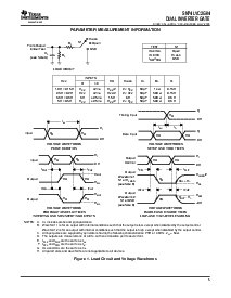
logicdiagram(positivelogic)
overoperatingfree-airtemperaturerange(unlessotherwisenoted)
MINMAXUNIT
V
CC
supplyvoltagerange–0.56.5v
V
I
Inputvoltagerange
(2)
–0.56.5v
V
O
voltagerangeappliedtoanyoutputinthehigh-impedanceorpower-offstate
(2)
–0.56.5v
V
O
Voltagerangeappliedtoanyoutputinthehighorlowstate
(2)(3)
–0.5v
CC
+0.5v
I
IK
InputclampcurrentV
I
<0–50ma
I
OK
OutputclampcurrentV
O
<0–50ma
I
O
Continuousoutputcurrent
±
50mA
ContinuouscurrentthroughV
CC
orGND
±
100mA
DBVpackage165
DCKpackage259
θ
JA
Packagethermalimpedance
(4)
°
c/w
yea/yzapackage143
yep/yzppackage123
T
stg
Storagetemperaturerange–65150
°
C
(1)stressesbeyondthoselistedunder"absolutemaximumratings"maycausepermanentdamagetothedevice.thesearestressratings
仅有的,andfunctionaloperationofthedeviceattheseoranyotherconditionsbeyondthoseindicatedunder"recommendedoperating
情况"isnotimplied.exposuretoabsolute-最大-ratedconditionsforextendedperiodsmayaffectdevicereliability.
(2)theinputnegative-voltageandoutputvoltageratingsmaybeexceedediftheinputandoutputcurrentratingsareobserved.
(3)thevalueofv
CC
isprovidedintherecommendedoperatingconditionstable.
(4)thepackagethermalimpedanceiscalculatedinaccordancewithjesd51-7.
2