www.德州仪器.com
RECEIVERSWITCHINGCHARACTERISTICS
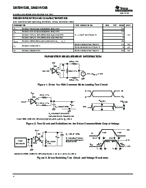
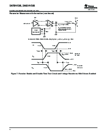
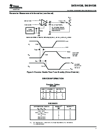
PARAMETERMEASUREMENTINFORMATION
60
Ω
±
1%
V
OD
0 或者 3 v
_
+
–7 v < v
(测试)
< 12 v
DE
V
CC
一个
B
D
375
Ω
±
1%
375
Ω
±
1%
V
OC
27
Ω
±
1%
输入
一个
B
V
一个
V
B
V
oc(pp)
∆
V
oc(ss)
V
OC
27
Ω
±
1%
C
L
= 50 pf
±
20%
D
一个
B
DE
V
CC
输入: prr = 500 khz, 50% 职责 循环,t
r
<6ns, t
f
<6ns, z
O
= 50
Ω
C
L
包含 fixture 和
仪器 电容
V
OD
R
L
= 54
Ω
±
1%
50
Ω
发生器: prr = 500 khz, 50% 职责 循环, t
r
<6 ns, t
f
<6 ns, z
o
= 50
Ω
t
PLH
t
PHL
1.5 v 1.5 v
3 v
≈
2 v
≈
–2 v
90%
10%
0 v
V
I
V
OD
t
r
t
f
C
L
= 50 pf
±
20%
C
L
包含 fixture
和 仪器
电容
D
一个
B
DE
V
CC
V
I
输入
发生器
90%
0 v
10%
sn75hvd08,sn65hvd08
SLLS550A–NOVEMBER2002–REVISEDMAY2003
overrecommendedoperatingconditionsunlessotherwisenoted
PARAMETERTESTCONDITIONSMINTYPMAXUNIT
t
PHL
receiverhigh-至-lowpropagationdelaytime70
t
PLH
receiverlow-至-highpropagationdelaytime70
t
r
receiver10%-至-90%differentialoutputrisetimec
L
=15pf,seefigure65ns
t
f
receiver90%-至-10%differentialoutputfalltime5
t
sk(p)
receiverdifferentialoutputpulseskew,|t
PHL
-t
PLH
|4.5
driverenabled,seefigure715ns
t
en
Receiverenabletime
driverdisabled,seefigure86µs
t
dis
receiverdisabletimedriverenabled,seefigure720ns
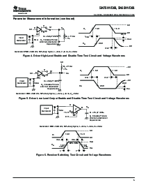
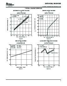
figure1.driverv
OD
withcommon-modeloadingtestcircuit
figure2.testcircuitanddefinitionsforthedrivercommon-modeoutputvoltage
figure3.driverswitchingtestcircuitandvoltagewaveforms
4