www.德州仪器.com
0
100
120
140
160
180
pcb 铜 范围 − 在
2
− 热的 阻抗 −
θ
JA
R c/w
°
非 空气 流动
80
60
40
20
0.1 1 10
1
2
3
4
5
0.1 1 10 100
铜 散热器 范围 − cm
2
T
一个
= 55
°
C
非 空气 流动
150 lfm
250 lfm
P
D
最大 (w)
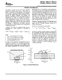
SOT223PowerDissipation
P
D
最大值
(
3.3
2.5
)
V x 1 一个
800 mW
(10)
R
θ
JA
最大值
(125
55)
°
C
800 mW
87.5
°
C
W
0
1
2
3
6
0 25 50 75 100 150125
T
一个
= 25
°
C
T
一个
(
°
c)
4
5
4 在
2
pcb 范围
0.5 在
2
pcb 范围
P
D
最大 (w)
tps79601,tps79618,tps79625
tps79628,tps79630,tps79633
SLVS351D–SEPTEMBER2002–REVISEDOCTOBER2004
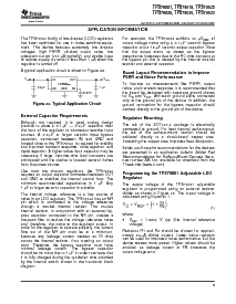
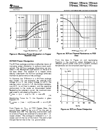
figure28.sot223thermalresistancevspcb
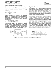
figure27.maximumpowerdissipationvscopper
范围
HeatsinkArea
FromthedatainFigure28andrearranging
equation6,themaximumpowerdissipationfora
differentgroundplaneareaandaspecificambient
TheSOT223packageprovidesaneffectivemeansof
temperaturecanbecomputed(seefigure29).
managingpowerdissipationinsurfacemountappli-
cations.thesot223packagedimensionsarepro-
videdinthe
MechanicalData
sectionattheendof
thedatasheet.theadditionofacopperplane
directlyunderneaththeSOT223packageenhances
thethermalperformanceofthepackage.
toillustrate,thetps72525inasot223package
waschosen.forthisexample,theaverageinput
voltageis3.3v,theoutputvoltageis2.5v,这
averageoutputcurrentis1a,theambienttempera-
ture55
°
c,noairflowispresent,andtheoperating
environmentisthesameasdocumentedbelow.
neglectingthequiescentcurrent,themaximumaver-
agepoweriscalculatedasequation10:
SubstitutingT
J
maxforT
J
intoEquation6gives
equation11:
(11)
fromfigure28,r
Θ
JA
vspcbcopperarea,这
figure29.sot223powerdissipation
groundplaneneedstobe0.55in
2
forthepartto
dissipate800mw.theoperatingenvironmentused
toconstructfigure28consistedofaboardwith1oz.
copperplanes.thepackageissolderedtoa1oz.
copperpadonthetopoftheboard.thepadistied
throughthermalviastothe1oz.groundplane.
13