www.德州仪器.com
tps726126/15/16
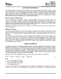
输出
在
地
EN
V
ref
电流 限制
/ 热的
保护
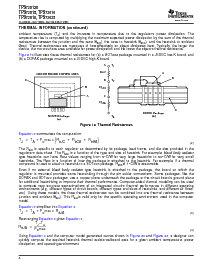
0.93
×
V
ref
Deglitch
和
延迟
重置
1.220
注释:一个. V
RES
是 这 最小 输入 电压 为 一个 有效的 重置.
在
V
RES
(看 便条 一个)
V
RES
t
t
t
输出
门槛
电压
重置
输出
200 ms
延迟
200 ms
延迟
输出
未阐明的
输出
未阐明的
V
它+
V
它−
V
它+
V
它−
TPS726126
tps72615,tps72616
tps72618,tps72625
SLVS403F–MAY2002–REVISEDMAY2005
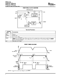
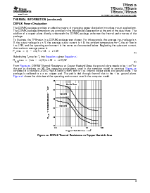
FUNCTIONALBLOCKDIAGRAM
TerminalFunctions
终端
描述
nameno.
GND3Ground
ENABLE1Enableinput
IN2Inputsupplyvoltage
reset5thisterminalistheresetoutput.whenusedwithapull-upresistor,thisopen-drainoutputprovidestheactivelow
resetsignalwhentheregulatoroutputvoltagedropsmorethan5%belowitsnominaloutputvoltage.thereset
delaytimeistypically200ms.
OUT4Regulatedoutputvoltage
RESETTIMINGDIAGRAM
4