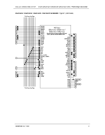
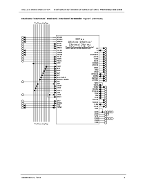
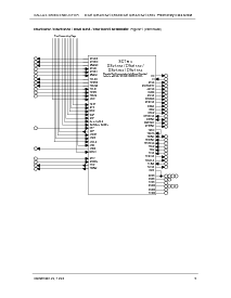
达拉斯市半导体 ds21q352/ds21q552/ds21q354/ds21q554 初步的 数据 薄板
12月 29, 1998 7
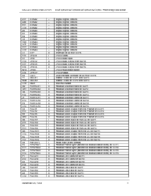
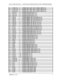
A17 DVSS2 – 数字的 信号 地面.
A20 DVSS2 – 数字的 信号 地面.
B11 DVSS2 – 数字的 信号 地面.
C13 DVSS2 – 数字的 信号 地面.
A5 DVSS3 – 数字的 信号 地面.
B7 DVSS3 – 数字的 信号 地面.
B9 DVSS3 – 数字的 信号 地面.
C3 DVSS3 – 数字的 信号 地面.
H20 DVSS4 – 数字的 信号 地面
L20 DVSS4 – 数字的 信号 地面
N17 DVSS4 – 数字的 信号 地面
U13 DVSS4 – 数字的 信号 地面
U1 INT* O 中断 为 所有 四 scts.
Y15 JTCLK I jtag 时钟.
N1 JTDI I jtag 数据 输入.
H18 JTDO2 O jtag 数据 输出 从 sct2.
V17 JTDO3 O jtag 数据 输出 从 sct3.
V19 JTDO4 O jtag 数据 输出 从 sct4.
W13 JTMS I jtag 测试 模式 选择.
V18 JTRST* I jtag 重置.
K2 LIUC I 线条 接口 连接 为 所有 四 scts.
T1 MCLK1 I 主控 时钟 为 sct1 和 sct3.
W20 MCLK2 I 主控 时钟 为 sct2 和 sct4.
U10 MUX I mux 总线 选择.
M2 RCHBLK1 O receive 频道 块 为 sct1.
G17 RCHBLK2 O receive 频道 块 为 sct2.
G4 RCHBLK3 O receive 频道 块 为 sct3.
Y12 RCHBLK4 O receive 频道 块 为 sct4.
J1 RCHCLK1 O receive 频道 时钟 为 sct1.
D14 RCHCLK2 O receive 频道 时钟 为 sct2.
F3 RCHCLK3 O receive 频道 时钟 为 sct3.
U14 RCHCLK4 O receive 频道 时钟 为 sct4.
N3 RCLK1 O receive 时钟 输出 从 这 framer 在 sct1.
B13 RCLK2 O receive 时钟 输出 从 这 framer 在 sct2.
E3 RCLK3 O receive 时钟 输出 从 这 framer 在 sct3.
M18 RCLK4 O receive 时钟 输出 从 这 framer 在 sct4.
M4 RCLKI1 I receive 时钟 输入 为 这 liu 在 sct1.
A15 RCLKI2 I receive 时钟 输入 为 这 liu 在 sct2.
A4 RCLKI3 I receive 时钟 输入 为 这 liu 在 sct3.
R17 RCLKI4 I receive 时钟 输入 为 这 liu 在 sct4.
M3 RCLKO1 O receive 时钟 输出 从 这 liu 在 sct1.
C14 RCLKO2 O receive 时钟 输出 从 这 liu 在 sct2.
B4 RCLKO3 O receive 时钟 输出 从 这 liu 在 sct3.
T17 RCLKO4 O receive 时钟 输出 从 这 liu 在 sct4.
N2 rd*(ds*) I 读 输入 (数据 strobe)
K4 RFSYNC1 O receive 框架 同步 (在之前这 receive elastic store) 为 sct1.
D17 RFSYNC2 O receive 框架 同步 (在之前这 receive elastic store) 为 sct2.
A2 RFSYNC3 O receive 框架 同步 (在之前这 receive elastic store) 为 sct3.
V14 RFSYNC4 O receive 框架 同步 (在之前这 receive elastic store) 为 sct4.
F1 RLCLK1 O receive link 时钟 为 sct1.
A12 RLCLK2 O receive link 时钟 为 sct2.
D3 RLCLK3 O receive link 时钟 为 sct3.
K18 RLCLK4 O receive link 时钟 为 sct4.
G2 RLINK1 O receive link 数据 为 sct1.
A13 RLINK2 O receive link 数据 为 sct2.
A3 RLINK3 O receive link 数据 为 sct3.
U12 RLINK4 O receive link 数据 为 sct4.