MUN2211T1 序列
9
motorola small–signal 晶体管, fets 和 二极管 设备 数据
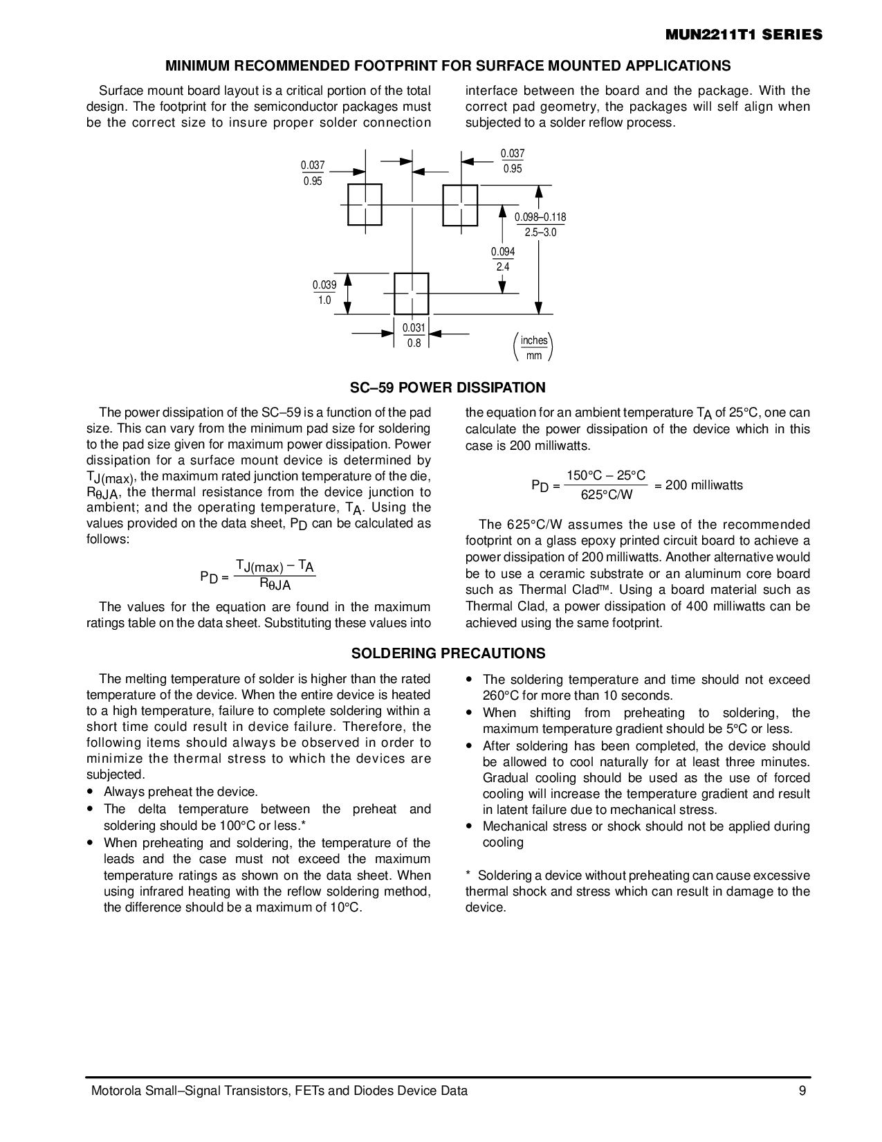
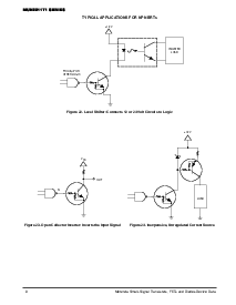
最小 推荐 footprint 为 表面 挂载 产品
表面挂载 板 布局 是 一个 核心的 portion 的 这总的
设计.这 footprint为 这 半导体 包装 必须
是the c或者rect size to insure proper solderconnection
interface between theboard一个nd the package. w它h the
准确无误的p一个d geometry, the packages will self 一个lign when
subjected 至 一个 焊盘 软熔焊接 处理.
mm
英寸
2.5–3.0
0.039
1.0
0.094
0.8
0.098–0.118
2.4
0.031
0.95
0.037
0.95
0.037
sc–59 电源 消耗
这电源 消耗 的 这 sc–59 是 一个 函数 的 这 垫子
大小.这个 能 相异 从 这 最小 垫子 大小 为 焊接
至 这 垫子 大小 给 为 最大 电源 消耗. 电源
消耗for 一个 surface mount device is determinedby
T
j(最大值)
,这 最大 评估 接合面 温度的 这 消逝,
R
θ
JA
,the thermal resistance from the device junction to
包围的;一个nd the operating temperature, t
一个
. usingthe
值提供 在 这 数据 薄板, p
D
能 是 计算 作
跟随:
P
D
=
T
j(最大值)
– t
一个
R
θ
JA
这values for the equation 一个re found in the maximum
比率表格 在 这 数据 薄板. substituting 这些 值 在
这 等式 为 一个 包围的 温度 t
一个
的 25
°
c, 一个 能
计算这 电源 消耗 的 这 设备 这个 在 这个
情况 是 200 毫瓦.
P
D
=
150
°
c – 25
°
C
625
°
c/w
= 200 毫瓦
这625
°
c/w 一个ssumes the use of the recommended
footprint在 一个 glass 环氧的 打印 电路 板至 达到 一个
电源消耗 的200 毫瓦. 另一 alternative 将
是至 使用 一个 陶瓷的 基质 或者 一个 铝 核心 板
此类一个s thermal clad
. using 一个 board material such 一个s
热的clad, 一个 电源 消耗 的 400毫瓦 能 是
达到 使用 这 一样 footprint.
焊接 预防措施
这melting 温度 的 焊盘 是 高等级的 比 这 评估
温度 的 这 设备. 当 这 全部 设备 是 heated
至一个 高 温度, 失败 至 完全 焊接 在里面 一个
短的time could result in device failure. therefore, the
followingitems should 一个lways be observedin order to
minimizethe therm一个l stress to which the devices 一个re
subjected.
•
总是 preheat 这 设备.
•
这delta 温度 在 这 preheat 和
焊接 应当 是 100
°
c 或者 较少.*
•
当preheating 和 焊接, 这 温度 的 这
leads和 这 情况 必须 不 超过 这 最大
温度比率 作 显示 在 这数据 薄板. 当
使用 infrared 加热 和 这 软熔焊接 焊接 方法,
这 区别 应当 是 一个 最大 的 10
°
c.
•
这焊接 温度 和 时间 应当 不 超过
260
°
c 为 更多 比 10 秒.
•
当shifting 从 preheating 至 焊接,这
最大 温度 gradient 应当 是 5
°
c 或者 较少.
•
之后焊接 有 被 完成,这 设备 应当
是允许 至cool naturally 为 在 least 三 分钟.
Gradual冷却 应当 是 使用 作 这 使用 的 强迫
冷却将 增加这 温度 gradient 和 结果
在 latent 失败 预定的 至 机械的 压力.
•
机械的压力或者 shock 应当 不 是 应用 在
冷却
* 焊接一个 设备 没有 preheating 能 导致 过度的
热的shock 和 压力 这个 能 结果 在 损坏 至 这
设备.