www.德州仪器.com
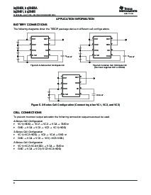
C
在
C
在
C
在
C
在
R
在
R
在
R
在
R
在
VC1
VC2
VC3
VC4
地
1.2 v (典型值)
CD
VDD
输出
I
CD
= 0.18
µ
一个 (典型值)
C
VD
C
延迟
R
VD
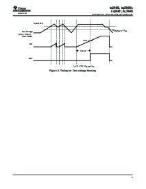
OVERVOLTAGEPROTECTION
DELAYTIMECALCULATION
t
d
1.2 V
C
(延迟)
I
CD
C
(延迟)
t
d
I
CD
1.2 V
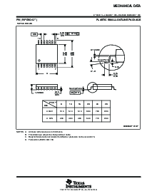
bq29400,bq29400a
bq29401,bq29405
SLUS568B–JULY2003–REVISEDNOVEMBER2004
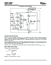
FUNCTIONALBLOCKDIAGRAM
WhenoneofthecellvoltagesexceedsV
(保护)
,aninternalcurrentsourcebeginstochargethecapacitor,
C
(延迟)
,connectedtothecdpin.ifthevoltageatthecdpin,v
cd,
reaches1.2v,theoutpinisactivatedand
transitionshigh.anexternallyconnectednchfetisactiviatedandblowstheexternalfuseinthepositive
batteryrail,seefigure1.
IfallcellvoltagesfallbelowV
(保护)
beforethevoltageatpincdreaches1.2v,thedelaytimedoesnotrun
输出.aninternalswitchclampsthecdpintogndanddischargesthecapacitor,c
(延迟)
,andsecuresthefull
delaytimeforthenextoccurringovervoltageevent.
oncethepinoutisactivated,ittransitionsbackfromhightolowafterallbatterycellsreachv
(保护)
-v
hys.
thedelaytimeiscalculatedasfollows:
WhereI
(cd)
=cdcurrentsource=0.18µa
4