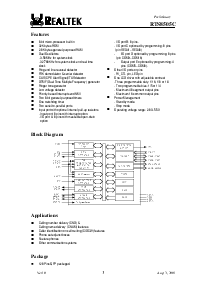
(前liminary)
RTS8505C
✂✁☎✄
1.0一个ug.3,2001
4
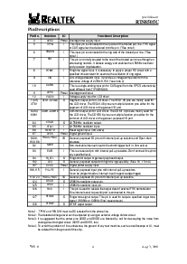
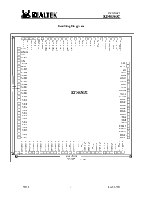
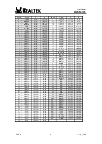
Pin 描述
Pin 非.
Notation i/o Functional descripti在
4
AVDD
电源 一个nalog power supply input
5
TIPIN
I This input pin is connected 至 the 德州仪器p 一侧 of the twistedpairline. fsk signal
or c作 signal c一个 是 delivered 在 this 管脚. (*see 便条 1)
6
RINGIN
I This input pin is connected 至 the ring 一侧 of the twisted pairline. (*see
不e 1)
7
RD1
I This pin isnormally coupled 至 这 一个 of the twisted pair 线s through 一个
一个ttenuating 网络. 它发现s 活力和 使能s the 3.58mhz oscillator
和 精确 环绕 发现.
8
RTIME
I Ring 时间 signal input. 它 isnecessary to apply一个 properrc circuit with 一个
specified 时间 constant for examine 这 validation of ring 信号.
9
VIN
I 低-voltage detector input. 它 provides一个 电压 comparator with 这
涉及 电压 of 2.45V±0.15v. (*see 便条 2)
10
CASIN
I This 是一个 单独的-ending input pin for c作 signal from the spcs, 改变natively
美国ed different from tipin/ringin.
11
一个VSS
电源 一个nalog 地面 input.
12
VLCD0
I Voltage supply input for lcd 驱动器
13-35,
37-61
SEG1
−
SEG48
O Segmentoutput pin for lcd 驱动器. theseg1-40 管脚s are mainly 美国ed for
the lcd 驱动器. the seg41-48 管脚s are 多样的 函数 管脚s either 为 the
segment 的 lcd 驱动r 或者 the generali/O端口
62-64,
69-81
COM1
−
COM16
O Comm在 output pin for lcd 驱动器. the com1-4 管脚s are mainly 美国ed for
the lcd 驱动器. the com5-16 管脚s are 多样的 函数 管脚s either for the
comm在 of lcd 驱动r 或者 the一般-purposedi/O端口
84
XTALO
O 32.768khz oscillatoroutput.
85
XTALI
I 32.768khz oscillator input.
86
RESETB
I Reset signal input. (low 起作用的)
87
DVSS
电源 Digital ground input.
88-91,
103-106
PIOA0
−
PIOA7
i/o General-purposedi/o 管脚s with internalpull-向上 电阻s和 打开-流
结构
92
NMIB
I 非-毫安skable interr向上t input withschmitt 触发ggerbuilt 在. (low 起作用的)
93 EAB I This 是一个 保留 管脚 和 internalpull-向上 电阻器. don’t connect this pin to
一个y specified 水平的.
94
ri_ctl
O Ring controloutput or一般-purposed output.
102
LED
O 一般-purposed output with 高 驱动 capability. (最大值.10 -15 毫安)
107
DVDD
电源 Digitalpower supply input
108-115
PI0
−
PI7
I
一般-purposed input 管脚s with internalpull-向上 电阻器
它 c一个 是 programmed 一个s interrupt input (负的-边缘 trigger)
116-123
PIOB0
−
PIOB7
i/o General-purposedi/o 管脚s with internalpull-向上 电阻器.
124
OSCO
O 3.58mhz oscillatoroutput 管脚.
125
OSCI
I 3.58mhz oscillator input 管脚.
126
RXD
I
This pin 是美国ed 至 receive 这 outputdat一个 of external fSKdemodulator.
One internal 串行-至-parallelport is connected 至 this 管脚.
127
RTONE
O Ringer t一个 signaloutput. this pin is 美国ed foroutput一个 指定 ringer t一个
信号. (1000Hz or1300Hz sine/ square 波)
128
DTONE
O DTMf signaloutput.
不e 1: ‘tipin’和 ‘ringin’ must是 dc isolated from the phoneline.
不e 2:The 发现 电压 level c一个 be调整ed by using 一个 external voltage 分隔r circuit.
不e 3:它 is suggested that the power 管脚s avdD和 dvdd are blocked by coil forde-coupling 这 噪音 from
analog circuit to digital circuit. (avSS和 dvSS, too)
不e 4:To 避免 这 problem ofline 不平衡, the 地面 of一个y test machine, such 一个s oscilloscope or 一个i, must
是 分开的 from the 地面 of this 碎片.