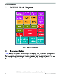
介绍
scf5250 整体的 coldfire® microprocessor 数据 薄板, rev. 1.1
freescale 半导体 3
1.2.3 增强 乘以 和 accumulate 单元 (emac)
这 整体的 emac 单位 提供 一个 一般 设置 的 dsp 行动 和 enhances这 integer 乘以
说明 在 这 coldfire architecture. 这 em交流 提供 符合实际在 三 related areas:
1. faster signed 和 unsigned integer multiplies
2. 新 乘以-accumulate 行动支承的 signed 和 unsigned operands
3. 新 miscellaneous 寄存器 行动
multiplies 的 16x16 和 32x32 with 48-位 accumulates 是supported 在 增加 至 一个 全部 设置 的 extensions
为 signed 和 unsigned integers pl美国 signed, fixed-要点fractional 输入 operands. 这 emac 有 一个
单独的-时钟 公布 为 32x32-位 multiplication instructions 和 实现一个 四-平台 执行
pipeline.
1.2.4 操作指南 cache
这 操作指南 cache improves 系统 效能 用供应 cached instructions 至 这 执行 单位
在 一个 单独的 时钟. 这 scf5250 processor 使用 一个 8k-字节, direct-编排 instructi在 cache 至 达到 107
mips 在 120 mhz. 这 cache 是 accessed 用 物理的 地址, 在哪里 各自16-字节 线条 组成 的 一个
地址 tag 和 一个 有效的 位. 这 instruction cache 也 包含 一个 bursting 接口 为 16-位 和 8-位 端口
sizes 至 quickly fill cache 线条.
1.2.5 内部的 128-kbyte sram
这 128-kbyte 在-碎片 sram 是 有 在 二banks, sram0 (64k) 和 sram1 (64k). 它 提供
一个 时钟-循环 进入 为 这 coldfire 核心. 这个 sram 能 store 处理器 堆栈 和 核心的 代号 或者
数据 部分 至 maximize效能. 记忆 在 sram1 能 是 accessed 下面 dma.
1.2.6 sdram 控制
这 scf5250 sdram 控制 提供 一个 glueless接口 为 一个 bank 的sdram 向上 至 32 mb (256
mbits). 这 控制 支持 一个 16-位 数据 总线. 一个 唯一的 addressing scheme 准许 为 增加 在
系统 记忆 大小 没有 rerouting 地址 线条 和 re线路 boards. 这 控制 运作 在 页
模式, 非-页 模式, 和 burst-页 模式 和 支持 sdrams.
1.2.7 系统 接口
这 scf5250 提供 一个 glueless interface 至 16-位 端口 size sram, 只读存储器, 和 peripheral 设备 和
独立 可编程序的 control 的 这 assertion 和 negation 的碎片-选择 和 写-使能 信号.
这 scf5250 也 支持 bursting roms.
1.2.8 外部 总线 接口
这 总线 接口 控制 transfers informati在 在 这 coldfire 核心 或者 dma 和 记忆,
peripherals, 或者 其它 设备s 在 这 外部 总线. 这 外部 总线 在terface 提供 23 位 的 地址 总线