www.德州仪器.com
_
+
V
DD
V
O+
V
O−
地
6
5
8
7
To 电池
C
s
IN−
IN+
4
3
R
I
R
I
40 k
Ω
40 k
Ω
+
−
C
I
C
I
C
F
C
F
C
一个
C
一个
R
一个
R
一个
(1)
C
(绕过)
是 optional
偏差
电路系统
2
关闭
1
C
(绕过)
(1)
100 k
Ω
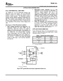
SelectingComponents
增益 = r
F
/r
I
(1)
f
c
1
2
R
I
C
I
(2)
-3 db
f
c
TPA6211A1
SLOS367B–AUGUST2003–REVISEDAUGUST2004
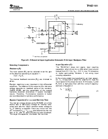
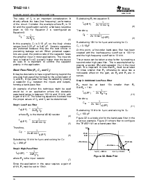
figure31.differentialinputapplicationschematicwithinputbandpassfilter
inputcapacitor(c
I
)
TheTPA6211A1doesnotrequireinputcoupling
电阻器(r
I
)
capacitorswhendrivenbyadifferentialinputsource
biasedfrom0.5vtov
DD
-0.8v.use1%tolerance
theinputresistor(r
I
)canbeselectedtosetthegain
orbettergain-settingresistorsifnotusinginput
oftheamplifieraccordingtoequation1.
couplingcapacitors.
inthesingle-endedinputapplication,aninputcapaci-
theinternalfeedbackresistors(r
F
)aretrimmedto
tor,c
I
,isrequiredtoallowtheamplifiertobiasthe
40k
Ω
.
inputsignaltotheproperdclevel.inthiscase,c
I
和
R
I
formahigh-passfilterwiththecornerfrequency
Resistormatchingisveryimportantinfullydifferential
definedinequation2.
放大器.thebalanceoftheoutputonthereference
voltagedependsonmatchedratiosoftheresistors.
cmrr,psrr,andthecancellationofthesecond
harmonicdistortiondiminishesifresistormismatch
occurs.因此,1%-toleranceresistorsorbetter
arerecommendedtooptimizeperformance.
bypasscapacitor(c
绕过
)andstart-uptime
TheinternalvoltagedividerattheBYPASSpinofthis
devicesetsamid-supplyvoltageforinternalrefer-
encesandsetstheoutputcommonmodevoltageto
V
DD
/2.addingacapacitorfiltersanynoiseintothis
管脚,increasingk
SVR
.c
(绕过)
alsodeterminestherise
timeofV
O+
andV
o-
whenthedeviceexitsshutdown.
thelargerthecapacitor,theslowertherisetime.
15