www.德州仪器.com
描述/orderinginformation(持续)
一个 Y
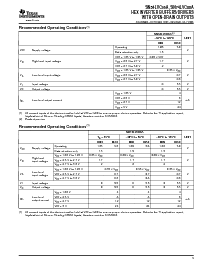
AbsoluteMaximumRatings
(1)
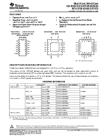
sn54lvc06a,sn74lvc06a
hexinverterbuffers/驱动器
withopen-drainoutputs
SCAS596N–OCTOBER1997–REVISEDJULY2005
thesedevicesarefullyspecifiedforpartial-电源-downapplicationsusingi
止
.thei
止
circuitrydisablesthe
输出,preventingdamagingcurrentbackflowthroughthedevicewhenitispowereddown.
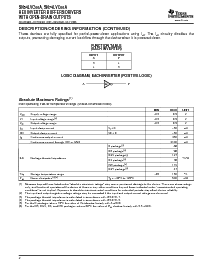
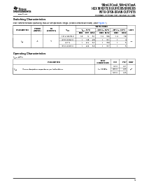
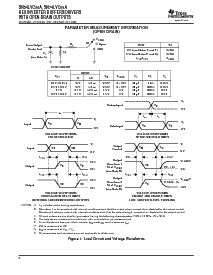
FUNCTIONTABLE
(eachinverter)
INPUTOUTPUT
AY
HL
LH
logicdiagram,eachinverter(positivelogic)
overoperatingfree-airtemperaturerange(unlessotherwisenoted)
MINMAXUNIT
V
CC
supplyvoltagerange–0.56.5v
V
I
Inputvoltagerange
(2)
–0.56.5v
V
O
outputvoltagerange–0.56.5v
I
IK
InputclampcurrentV
I
<0–50ma
I
OK
OutputclampcurrentV
O
<0–50ma
I
O
Continuousoutputcurrent
±
50mA
ContinuouscurrentthroughV
CC
orGND
±
100mA
Dpackage
(3)
86
DBpackage
(3)
96
DGVpackage
(3)
127
θ
JA
Packagethermalimpedance
°
c/w
NSpackage
(3)
76
PWpackage
(3)
113
RGYpackage
(4)
47
T
stg
Storagetemperaturerange–65150
°
C
P
tot
Powerdissipation
(5)(6)
T
一个
=–40
°
Cto125
°
C500mW
(1)stressesbeyondthoselistedunder"absolutemaximumratings"maycausepermanentdamagetothedevice.thesearestressratings
仅有的,andfunctionaloperationofthedeviceattheseoranyotherconditionsbeyondthoseindicatedunder"recommendedoperating
情况"isnotimplied.exposuretoabsolute-最大-ratedconditionsforextendedperiodsmayaffectdevicereliability.
(2)theinputandoutputnegative-voltageratingsmaybeexceedediftheinputandoutputcurrentratingsareobserved.
(3)thepackagethermalimpedanceiscalculatedinaccordancewithjesd51-7.
(4)thepackagethermalimpedanceiscalculatedinaccordancewithjesd51-5.
(5)forthedpackage:above70
°
CthevalueofP
tot
derateslinearlywith8mw/k.
(6)forthedb,dgv,ns,andpwpackages:above60
°
CthevalueofP
tot
derateslinearlywith5.5mw/k.
2