www.德州仪器.com
APPLICATIONINFORMATION
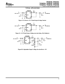
ADJUSTABLEOUTPUTVOLTAGEVERSION
V
输出
0.5 V
1
R1
R2
C1
1
2
10 kHz
R1
C2
R1
R2
C1
V
I
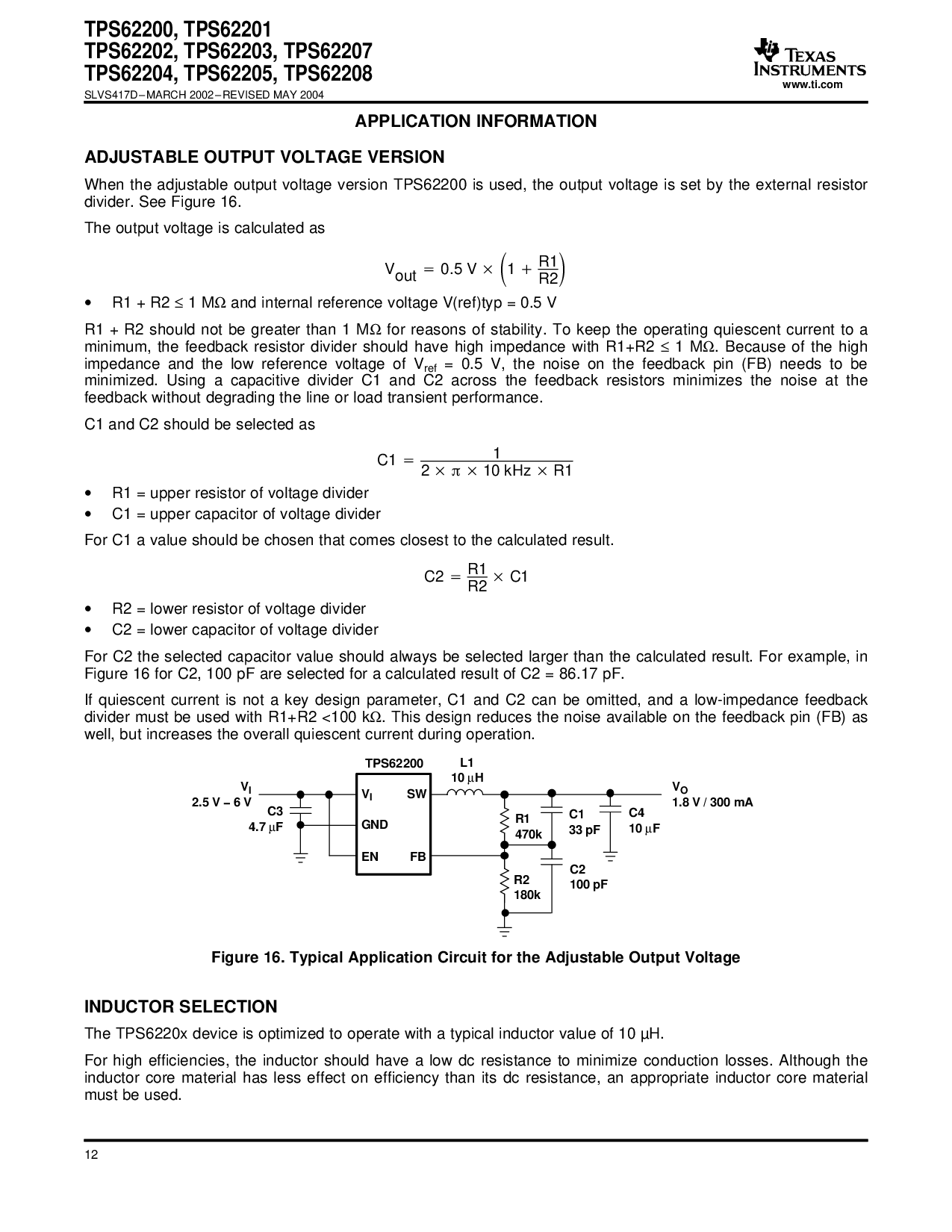
地
EN
SW
FB
C3
4.7
µ
F
L1
10
µ
H
C4
10
µ
F
TPS62200
V
I
2.5 v − 6 v
V
O
1.8 v / 300 毫安
R1
470k
R2
180k
C1
33 pf
C2
100 pf
INDUCTORSELECTION
tps62200,tps62201
tps62202,tps62203,tps62207
tps62204,tps62205,tps62208
SLVS417D–MARCH2002–REVISEDMAY2004
whentheadjustableoutputvoltageversiontps62200isused,theoutputvoltageissetbytheexternalresistor
分隔物.seefigure16.
Theoutputvoltageiscalculatedas
•
R1+R2
≤
1M
Ω
andinternalreferencevoltagev(ref)典型值=0.5v
R1+R2shouldnotbegreaterthan1M
Ω
forreasonsofstability.tokeeptheoperatingquiescentcurrenttoa
最小,thefeedbackresistordividershouldhavehighimpedancewithr1+r2
≤
1M
Ω
.becauseofthehigh
impedanceandthelowreferencevoltageofV
ref
=0.5v,thenoiseonthefeedbackpin(fb)needstobe
使减少到最低限度.usingacapacitivedividerc1andc2acrossthefeedbackresistorsminimizesthenoiseatthe
feedbackwithoutdegradingthelineorloadtransientperformance.
C1andC2shouldbeselectedas
•
R1=upperresistorofvoltagedivider
•
C1=uppercapacitorofvoltagedivider
forc1avalueshouldbechosenthatcomesclosesttothecalculatedresult.
•
R2=lowerresistorofvoltagedivider
•
C2=lowercapacitorofvoltagedivider
forc2theselectedcapacitorvalueshouldalwaysbeselectedlargerthanthecalculatedresult.forexample,在
figure16forc2,100pfareselectedforacalculatedresultofc2=86.17pf.
ifquiescentcurrentisnotakeydesignparameter,c1andc2canbeomitted,andalow-impedancefeedback
dividermustbeusedwithr1+r2<100k
Ω
.thisdesignreducesthenoiseavailableonthefeedbackpin(fb)作
好,butincreasestheoverallquiescentcurrentduringoperation.
figure16.typicalapplicationcircuitfortheadjustableoutputvoltage
thetps6220xdeviceisoptimizedtooperatewithatypicalinductorvalueof10µh.
forhighefficiencies,theinductorshouldhavealowdcresistancetominimizeconductionlosses.althoughthe
inductorcorematerialhaslesseffectonefficiencythanitsdcresistance,anappropriateinductorcorematerial
mustbeused.
12