PZTA14T1
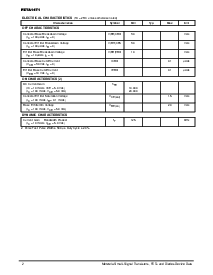
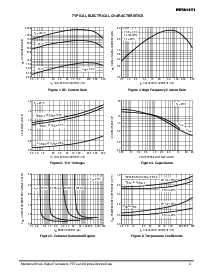
4
motorola small–signal 晶体管, fets 和 二极管 设备 数据
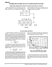
信息 为 使用 这 sot-223 表面 挂载 包装
最小 推荐 footprint 为 表面 挂载 产品
表面挂载 板 布局 是 一个 核心的 portion 的 这总的
设计.这 footprint为 这 半导体 包装 必须
是the correct size to insure proper solderconnection
interface between theboard一个nd the package. w它h the
准确无误的p一个d geometry, the packages will self 一个lign when
subjected 至 一个 焊盘 软熔焊接 处理.
0.079
2.0
0.15
3.8
0.248
6.3
0.079
2.0
0.059
1.5
0.059
1.5
0.059
1.5
0.091
2.3
mm
英寸
0.091
2.3
sot-223
sot-223 电源 消耗
这电源 消耗 的 这 sot-223 是 一个 函数 的 这
垫子size. This c一个n vary from the minimum p一个d size f或者
焊接至 一个 垫子 大小 给 为 最大 电源 消耗.
电源消耗 为 一个表面 挂载 设备 是 决定
用 t
j(最大值)
, 这 最大评估 接合面 温度 的 这
消逝, r
θ
JA
, 这 热的 阻抗 从 这 设备 接合面 至
包围的,一个nd the operating temperature, t
一个
. usingthe
值提供 在 这 数据 薄板 为 这 sot-223 包装,
P
D
能 是 计算 作 跟随:
P
D
=
T
j(最大值)
– t
一个
R
θ
JA
这values for the equation 一个re found in the maximum
比率表格 在 这 数据 薄板. substituting 这些 值 在
这 等式 为 一个 包围的 温度 t
一个
的 25
°
c, 一个 能
计算这 电源 消耗 的 这 设备 这个 在 这个
情况 是 1.5 watts.
P
D
=
150
°
c – 25
°
C
83.3
°
c/w
= 1.5 watts
这 83.3
°
c/w 为 这 sot-223 包装 假设 这 使用
的这 推荐 footprint 在 一个 glass 环氧的 打印 电路
板 至 达到 一个 电源 消耗 的 1.5 watts. 那里 是
其它 alternatives 至 实现 高等级的 电源 消耗 从
这SOT-223包装. 一个 是 至 增加 这 范围 的 这
集电级垫子. 用 增加 这 范围 的 这 集电级 垫子, 这
电源dissipation c一个n be increased.一个lthough the power
消耗能 almost 是 doubled 和 这个 方法, 范围是
带去向上 在 这 打印 电路 板 这个 能 defeat 这
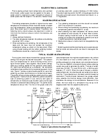
目的的 使用 表面 挂载 技术. 一个图表 的 r
θ
JA
相比 集电级 垫子 范围 是 显示 在 图示 7.
0.8 watts
1.25 watts*
1.5 watts
R , 热的 阻抗, 接合面
至 包围的 ( c/w)
θ
JA
°
一个, 范围 (正方形的 英寸)
0.0 0.2 0.4 0.6 0.8 1.0
160
140
120
100
80
图示 7. 热的 阻抗 相比 集电级
垫子 范围 为 这 sot-223 包装 (典型)
板 材料 = 0.0625
″
g-10/fr-4, 2 oz 铜
T
一个
= 25
°
C
*mounted 在 这 dpak footprint
另一alternative 将 是 至 使用 一个 陶瓷的 基质 或者
一个铝 核心 板 此类 作 热的 clad
. 使用 一个
板material such 一个s thermal clad, 一个n 一个luminum core
板,这 电源 消耗 能 是 doubled 使用 这 一样
footprint.