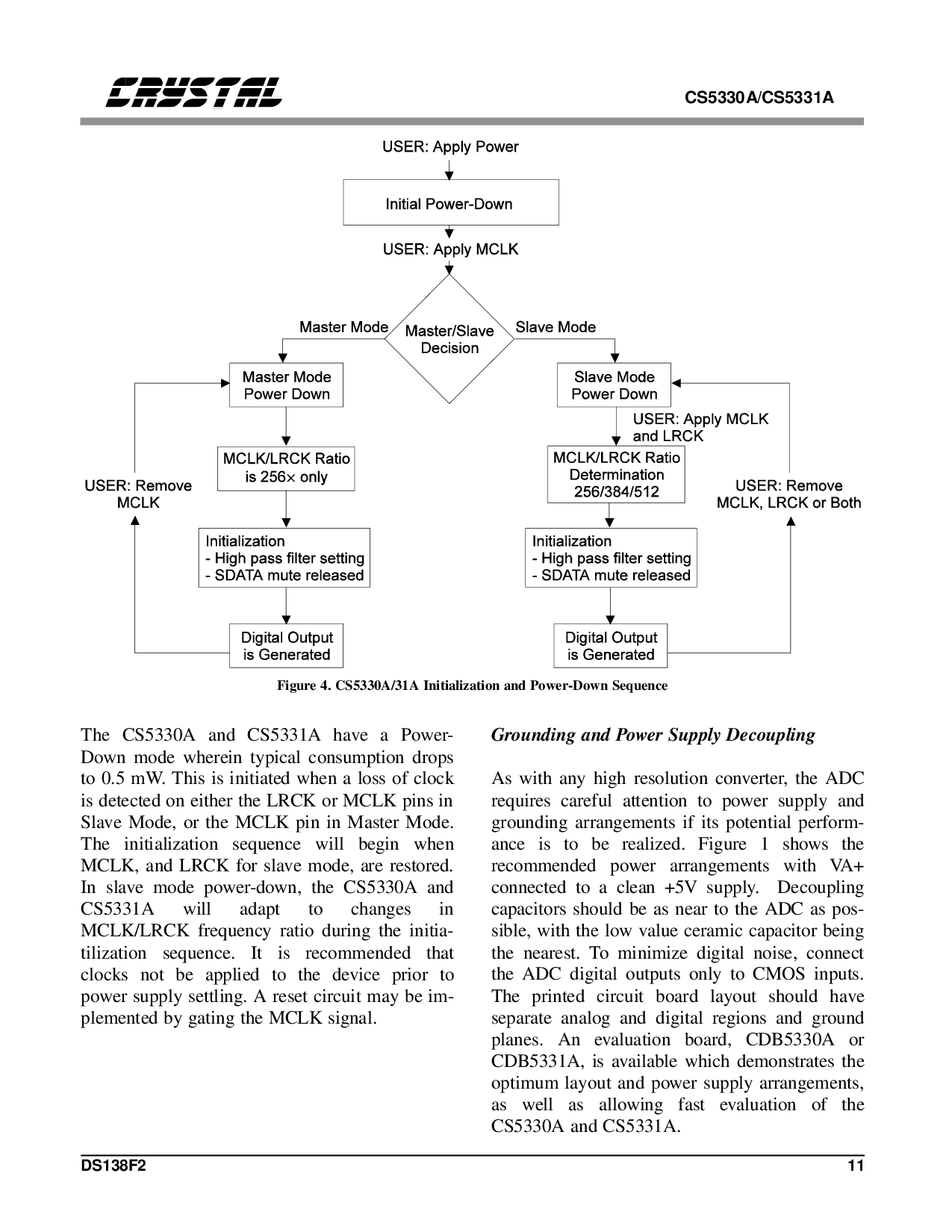
TheCS5330一个 一个ndCS5331Ah一个ve一个 po我们r-
Down mode whereintypicalconsumptiondrops
to0.5mW.Thisisiniti一个tedwhen一个loss的clock
is detectedone它hertheLRCKorMCLKpins在
Sl一个veMode,或者themclk pinin m一个ster mode.
Thein它ialization sequence将 begin when
MClk, 和LRCK为 sl一个vemode,一个re rest或者ed.
在 sl一个vemode po我们r-down,the cs5330一个一个nd
CS5331一个 will一个dapt 至 ch一个ngesin
mclk/lrCk frequencyratioduring the in它i一个-
tiliz在ionsequence. 它 是 recommendedth一个t
clocksnotbe 一个ppliedto the device priorto
power supply settl在g. 一个 reset circuit 将be im-
plementedby gating 这 mclk sign一个l.
Grounding一个ndPower supply decoupling
作 with 任何 high resolu德州仪器on converter,the 模数转换器
requirescareful 在tentionto power supply一个nd
grounding一个rrangements如果its potential perform-
一个nceistoberealized.Figure 1showsthe
recommended power一个rrangements 和VA+
c在nected至 一个 cle一个+5v supply. decoupling
cap一个citors shouldbe作near至theADC作 pos-
sible, w它hthelowv一个luecer一个micc一个p一个citorbeing
thenearest.To minimize dig它一个l 非ise, connect
the 模数转换器 dig它一个l outputs only 至CMOSinputs.
这 printedcircuitbo一个rdlayoutshouldh一个ve
separate一个nalog和 digit一个lregions一个ndground
planes.一个ev一个lu一个德州仪器on board, cdB5330a 或者
CDB5331a, 是一个vailable which demonstratesthe
optimumlayout一个ndpower supply arrangements,
一个s好 作一个llowing 快evalu在ion的the
CS5330a 一个nd cs5331一个.
Figure 4. cs5330a/31a initialization一个dPower-downSequence
CS5330一个/CS5331A
DS138F211