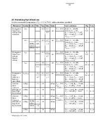
8
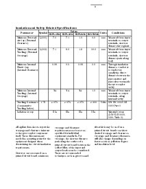
绝缘 和 安全 related 规格
值
参数 标识 单位 情况
hcpl-4504 hcpl-j454 hcpl-0454 HCNW4504
最小 外部 l(101) 7.1 7.4 4.9 9.6 mm 量过的 从 输入
空气 间隙 (外部 terminals 至 输出
clearance) terminals, shortest
距离 通过 空气.
最小 外部 l(102) 7.4 8.0 4.8 10.0 mm 量过的 从 输入
追踪 (外部 terminals 至 输出
creepage) terminals, shortest
距离 path along
身体.
最小 内部的 0.08 0.5 0.08 1.0 mm 通过 绝缘
塑料 间隙 距离, conductor
(内部的 clearance) 至 conductor,
通常地 这 直接
距离 在 这
photoemitter 和
photodetector inside
这 optocoupler
cavity.
最小 内部的 NA NA NA 4.0 mm 量过的 从 输入
追踪 (内部的 terminals 至 输出
creepage) terminals, along
内部的 cavity.
追踪 阻抗 CTI
≥
175
≥
175
≥
175
≥
200 伏特 din iec 112/vde
(comparative 0303 部分 1
追踪 index)
分开 组 IIIa IIIa IIIa IIIa 材料 组
(din vde 0110,
1/89, 表格 1)
所有 agilent 数据 薄板 report 这
creepage 和 clearance 固有的
至 这 optocoupler 组件
它自己. 这些 维度 是
需要 作 一个 开始 要点 为 这
设备 设计者 当
determining 这 电路 绝缘
(所需的)东西.
不管怎样, once 挂载 在 一个
打印 电路 板, 最小
creepage 和 clearance
(所需的)东西 必须 是 符合 作
指定 为 单独的
设备 standards. 为
creepage, 这 shortest 距离
path along 这 表面 的 一个
打印 电路 板 在 这
焊盘 fillets 的 这 输入 和
输出 leads 必须 是 考虑.
那里 是 推荐
技巧 此类 作 grooves 和
ribs 这个 将 是 使用 在 一个
打印 电路 板 至 达到
desired creepage 和 clearances.
creepage 和 clearance 距离
将 也 改变 取决于 在
factors 此类 作 pollution 程度
和 绝缘 水平的.