MTD6N20E
5
motorola tmos 电源 场效应晶体管 晶体管 设备 数据
V
DS
, drain–to–source 电压 (伏特)
V
GS
, gate–to–source 电压 (伏特)
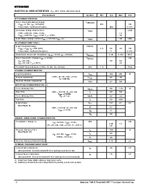
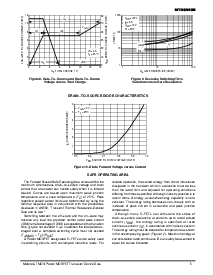
drain–to–source 二极管 特性
V
SD
, source–to–drain 电压 (伏特)
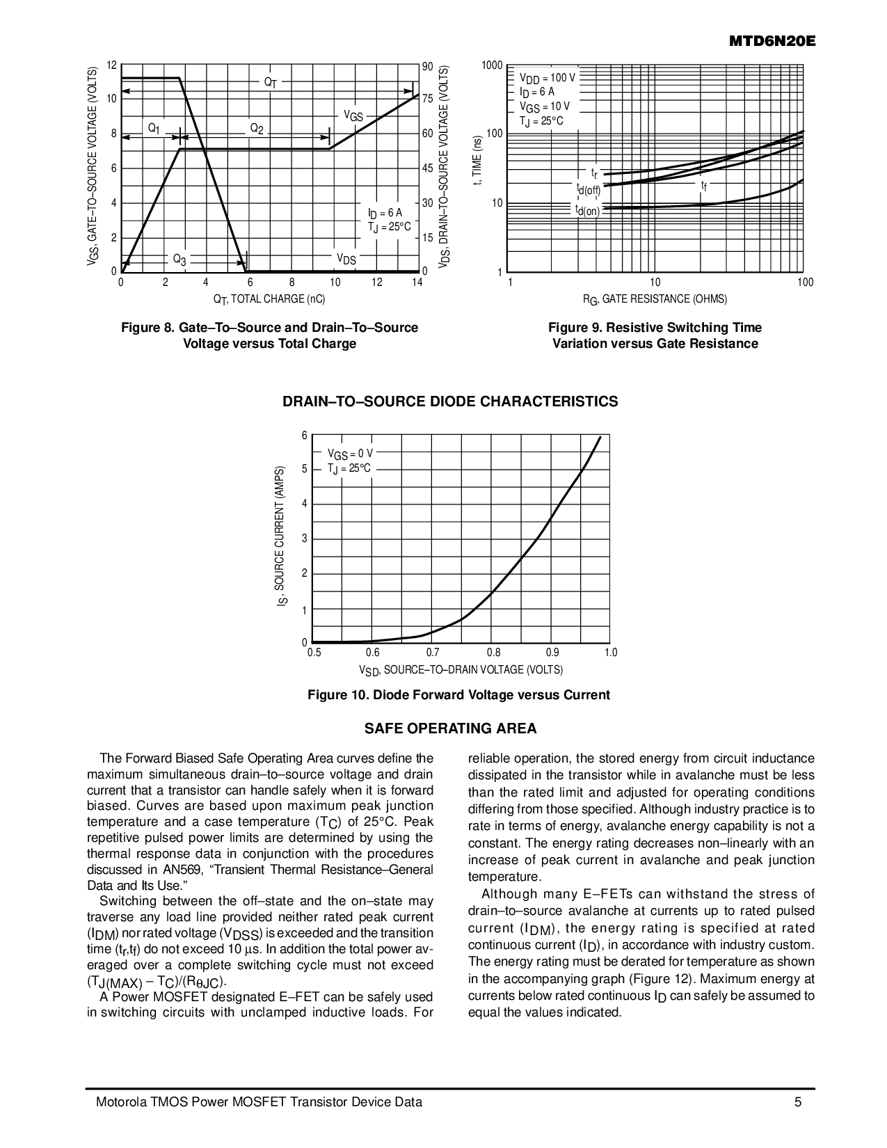
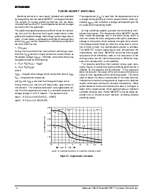
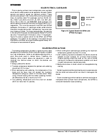
图示 8. gate–to–source 和 drain–to–source
电压 相比 总的 承担
I
S
, 源 电流 (放大器)
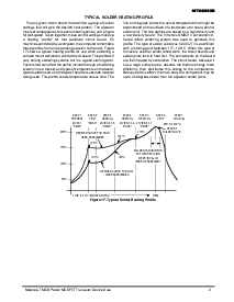
图示 9. resistive 切换 时间
变化 相比 门 阻抗
R
G
, 门 阻抗 (ohms)
t, 时间 (ns)
V
DD
= 100 v
I
D
= 6 一个
V
GS
= 10 v
T
J
= 25
°
C
t
d(止)
V
GS
= 0 v
T
J
= 25
°
C
图示 10. 二极管 向前 电压 相比 电流
Q
T
, 总的 承担 (nc)
t
f
t
d(在)
12
10
8
6
4
2
0
14121086420
1000
100
10
1
100101
90
75
60
45
30
15
0
6
5
4
3
2
1
0
0.5 0.6 0.7 0.8 0.9 1.0
I
D
= 6 一个
T
J
= 25
°
C
Q
T
V
DS
V
GS
Q
1
Q
2
Q
3
t
r
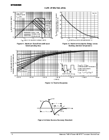
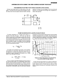
safe 运行 范围
这 向前 片面的 safe 运行 范围 曲线 定义 这
最大同时发生的 drain–to–source 电压 和 流
电流that一个 transistor c一个n handle safely when it is forward
片面的.Curves 一个re based upon maximum peak junction
temperature 一个nd 一个 c作e temperature (T
C
) of 25
°
C. peak
repetitive搏动 电源 限制 是 决定 用 使用 这
thermal response d在一个 in conjunction w它h the procedures
discussedin 一个n569,“Transient thermal resistance–General
数据 和 它的 使用.”
切换between the off–state 一个nd the on–state may
traverse任何 加载 线条 提供 neither 评估 顶峰 电流
(i
DM
)也不 评估 电压 (v
DSS
) 是 超过 和 这 转变
时间 (t
r
,t
f
) 做 不 超过 10
µ
s. 在 增加 这 总的 电源 av-
eragedover 一个 complete switching cyclem美国t not exceed
(t
j(最大值)
– t
C
)/(r
θ
JC
).
一个电源 场效应晶体管 designated e–fet 能 是 safely 使用
在 切换circuitsw它h unclamped inductive loads. f或者
可依靠的运作, 这贮存 活力 从 电路 电感
dissipated在 这晶体管 当 在 avalanche 必须 是 较少
比the rated limit 一个nd 一个djusted for operating conditions
differing从 那些 指定.虽然 工业 实践 是 至
比率在 条款 的活力, avalanche 活力 能力 是 不 一个
常量.这 活力 比率 减少 non–linearly 和一个
增加of peak current in 一个valanche一个nd peak junction
温度.
一个lthoughm一个y e–FETs c一个n withst一个d the stress of
drain–to–source一个valanche 一个t currents up to rated pulsed
current(I
DM
),the energy r一个ting is specified 一个t r一个ted
持续的 电流 (i
D
), 在 一致 和 工业 custom.
这活力 比率 必须 是 derated 为 温度 作 显示
在这 accompanying 图表 (图示 12). 最大 活力 在
电流在下 评估 持续的 i
D
能 safely是 assumed 至
equal 这 值 表明.